

12.5.3
Heterojunction solar cells
The third high efficiency concept is the silicon heterojunction (SHJ) solar cell. Before we
discuss the technological details, we briefly recall the principles of heterojunctions that
were discussed in Section 8.2.
Homojunctions, which are present in all the c-Si solar cell types discussed so far in
this chapter, are fabricated by different doping types within the same semiconductor
material. Hence, the bandgap in the p- and n-regions is the same. A junction consisting of
a p-doped semiconductor material and an n-doped semiconductor made from another
material is called a heterojunction. In SHJ cells, the heterojunction is formed in-between
two different silicon-based semiconductor materials. On the one hand, we use an n-type
float zone monocrystalline silicon wafer. The other material is hydrogenated amorphous
silicon (a-Si:H), which we will discuss in more detail in Section 13.3. a-Si:H is a silicon
material in which the atoms are not ordered in a crystalline lattice but in a disordered
lattice. For the moment we must only keep in mind that a-Si:H has a bandgap of around
1.7 eV which is considerably higher than that of c-Si (1.12 eV).
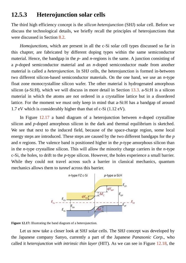
In Figure 12.17 a band diagram of a heterojunction between n-doped crystalline
silicon and p-doped amorphous silicon in the dark and thermal equilibrium is sketched.
We see that next to the induced field, because of the space-charge region, some local
energy steps are introduced. These steps are caused by the two different bandgaps for the p
and n regions. The valence band is positioned higher in the p-type amorphous silicon than
in the n-type crystalline silicon. This will allow the minority charge carriers in the n-type
c-Si, the holes, to drift to the p-type silicon. However, the holes experience a small barrier.
While they could not travel across such a barrier in classical mechanics, quantum
mechanics allows them to tunnel across this barrier.
Figure 12.17: Illustrating the band diagram of a heterojunction.
Let us now take a closer look at SHJ solar cells. The SHJ concept was developed by
the Japanese company Sanyo, currently a part of the Japanese Panasonic Corp., who
called it heterojunction with intrinsic thin layer (HIT). As we can see in Figure 12.18, the
Heterojunction solar cells
The third high efficiency concept is the silicon heterojunction (SHJ) solar cell. Before we
discuss the technological details, we briefly recall the principles of heterojunctions that
were discussed in Section 8.2.
Homojunctions, which are present in all the c-Si solar cell types discussed so far in
this chapter, are fabricated by different doping types within the same semiconductor
material. Hence, the bandgap in the p- and n-regions is the same. A junction consisting of
a p-doped semiconductor material and an n-doped semiconductor made from another
material is called a heterojunction. In SHJ cells, the heterojunction is formed in-between
two different silicon-based semiconductor materials. On the one hand, we use an n-type
float zone monocrystalline silicon wafer. The other material is hydrogenated amorphous
silicon (a-Si:H), which we will discuss in more detail in Section 13.3. a-Si:H is a silicon
material in which the atoms are not ordered in a crystalline lattice but in a disordered
lattice. For the moment we must only keep in mind that a-Si:H has a bandgap of around
1.7 eV which is considerably higher than that of c-Si (1.12 eV).
In Figure 12.17 a band diagram of a heterojunction between n-doped crystalline
silicon and p-doped amorphous silicon in the dark and thermal equilibrium is sketched.
We see that next to the induced field, because of the space-charge region, some local
energy steps are introduced. These steps are caused by the two different bandgaps for the p
and n regions. The valence band is positioned higher in the p-type amorphous silicon than
in the n-type crystalline silicon. This will allow the minority charge carriers in the n-type
c-Si, the holes, to drift to the p-type silicon. However, the holes experience a small barrier.
While they could not travel across such a barrier in classical mechanics, quantum
mechanics allows them to tunnel across this barrier.
Figure 12.17: Illustrating the band diagram of a heterojunction.
Let us now take a closer look at SHJ solar cells. The SHJ concept was developed by
the Japanese company Sanyo, currently a part of the Japanese Panasonic Corp., who
called it heterojunction with intrinsic thin layer (HIT). As we can see in Figure 12.18, the