

12.3
how to fabricate polysilicon. We have seen that monocrystalline ingots are made using
either the Czochralski or the float-zone process, while multicrystalline ingots are made
using a casting method. Wafers are fabricated by sawing these ingots. A method that does
not have any kerf losses is the ribbon silicon approach.
Designing c-Si solar cells
In this section, we briefly discuss the operating principles of c-Si solar cells. In particular,
we discuss several technical aspects that play an important role in the collection of the
light, excitation of charge carriers, and the reduction of optical losses.
In Chapter 8 we discussed how an illuminated p-n junction can operate as a solar cell.
In the illustrations used there, both the p-doped and n-doped regions have the same
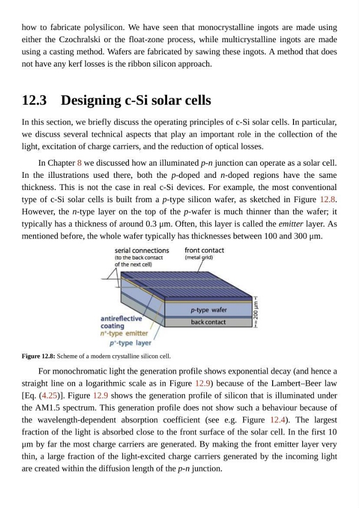
thickness. This is not the case in real c-Si devices. For example, the most conventional
type of c-Si solar cells is built from a p-type silicon wafer, as sketched in Figure 12.8.
However, the n-type layer on the top of the p-wafer is much thinner than the wafer; it
typically has a thickness of around 0.3 μm. Often, this layer is called the emitter layer. As
mentioned before, the whole wafer typically has thicknesses between 100 and 300 μm.
Figure 12.8: Scheme of a modern crystalline silicon cell.
For monochromatic light the generation profile shows exponential decay (and hence a
straight line on a logarithmic scale as in Figure 12.9) because of the Lambert–Beer law
[Eq. (4.25)]. Figure 12.9 shows the generation profile of silicon that is illuminated under
the AM1.5 spectrum. This generation profile does not show such a behaviour because of
the wavelength-dependent absorption coefficient (see e.g. Figure 12.4). The largest
fraction of the light is absorbed close to the front surface of the solar cell. In the first 10
μm by far the most charge carriers are generated. By making the front emitter layer very
thin, a large fraction of the light-excited charge carriers generated by the incoming light
are created within the diffusion length of the p-n junction.
how to fabricate polysilicon. We have seen that monocrystalline ingots are made using
either the Czochralski or the float-zone process, while multicrystalline ingots are made
using a casting method. Wafers are fabricated by sawing these ingots. A method that does
not have any kerf losses is the ribbon silicon approach.
Designing c-Si solar cells
In this section, we briefly discuss the operating principles of c-Si solar cells. In particular,
we discuss several technical aspects that play an important role in the collection of the
light, excitation of charge carriers, and the reduction of optical losses.
In Chapter 8 we discussed how an illuminated p-n junction can operate as a solar cell.
In the illustrations used there, both the p-doped and n-doped regions have the same
thickness. This is not the case in real c-Si devices. For example, the most conventional
type of c-Si solar cells is built from a p-type silicon wafer, as sketched in Figure 12.8.
However, the n-type layer on the top of the p-wafer is much thinner than the wafer; it
typically has a thickness of around 0.3 μm. Often, this layer is called the emitter layer. As
mentioned before, the whole wafer typically has thicknesses between 100 and 300 μm.
Figure 12.8: Scheme of a modern crystalline silicon cell.
For monochromatic light the generation profile shows exponential decay (and hence a
straight line on a logarithmic scale as in Figure 12.9) because of the Lambert–Beer law
[Eq. (4.25)]. Figure 12.9 shows the generation profile of silicon that is illuminated under
the AM1.5 spectrum. This generation profile does not show such a behaviour because of
the wavelength-dependent absorption coefficient (see e.g. Figure 12.4). The largest
fraction of the light is absorbed close to the front surface of the solar cell. In the first 10
μm by far the most charge carriers are generated. By making the front emitter layer very
thin, a large fraction of the light-excited charge carriers generated by the incoming light
are created within the diffusion length of the p-n junction.