

where J 0 is the saturation current density of the p-n junction, given by
Equation (8.23) is known as the Shockley equation that describes the current–voltage
behaviour of an ideal p-n diode. It is a fundamental equation for microelectronics device
physics. The saturation current density is also known as dark current density; its detailed
derivation for the p-n junction is carried out in Appendix B.1. The saturation-current
density is given by
The saturation current density depends in a complex way on the fundamental
semiconductor parameters. Ideally the saturation current density should be as low as
possible and this requires an optimal and balanced design of the p-type and n-type
semiconductor properties. For example, an increase in the doping concentration decreases
the diffusion length of the minority carriers, which means that the optimal product of these
two quantities requires a delicate balance between these two properties.
The recombination of the majority carriers due to the diffusion of the injected
minority carriers into the bulk of the quasi-neutral regions results in a lowering of the
concentration of the majority carriers compared to the one under equilibrium. The drop in
the concentration of the majority carriers is balanced by the flow of the majority carriers
from the electrodes into the bulk. In this way the net current flows through the p-n
junction under forward-bias voltage. For high reverse-bias voltage, the Boltzmann factor
in Eq. (8.23) becomes very small and can be neglected. The net current density is given by
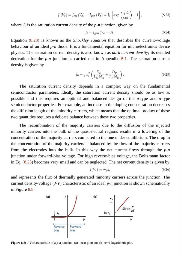
and represents the flux of thermally generated minority carriers across the junction. The
current density-voltage (J-V) characteristic of an ideal p-n junction is shown schematically
in Figure 8.8.
Figure 8.8: J-V characteristic of a p-n junction; (a) linear plot; and (b) semi-logarithmic plot.
Equation (8.23) is known as the Shockley equation that describes the current–voltage
behaviour of an ideal p-n diode. It is a fundamental equation for microelectronics device
physics. The saturation current density is also known as dark current density; its detailed
derivation for the p-n junction is carried out in Appendix B.1. The saturation-current
density is given by
The saturation current density depends in a complex way on the fundamental
semiconductor parameters. Ideally the saturation current density should be as low as
possible and this requires an optimal and balanced design of the p-type and n-type
semiconductor properties. For example, an increase in the doping concentration decreases
the diffusion length of the minority carriers, which means that the optimal product of these
two quantities requires a delicate balance between these two properties.
The recombination of the majority carriers due to the diffusion of the injected
minority carriers into the bulk of the quasi-neutral regions results in a lowering of the
concentration of the majority carriers compared to the one under equilibrium. The drop in
the concentration of the majority carriers is balanced by the flow of the majority carriers
from the electrodes into the bulk. In this way the net current flows through the p-n
junction under forward-bias voltage. For high reverse-bias voltage, the Boltzmann factor
in Eq. (8.23) becomes very small and can be neglected. The net current density is given by
and represents the flux of thermally generated minority carriers across the junction. The
current density-voltage (J-V) characteristic of an ideal p-n junction is shown schematically
in Figure 8.8.
Figure 8.8: J-V characteristic of a p-n junction; (a) linear plot; and (b) semi-logarithmic plot.