

7.6
(a)
(b)
(c)
(d)
(e)
(f)
(g)
(h)
7.7
7.8
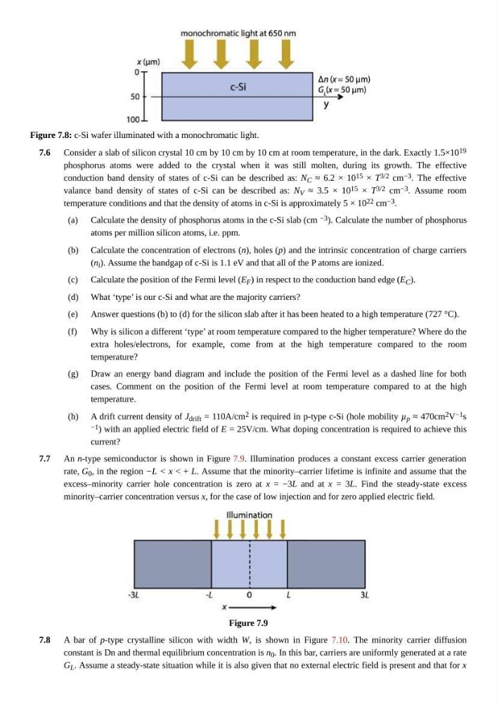
Figure 7.8: c-Si wafer illuminated with a monochromatic light.
Consider a slab of silicon crystal 10 cm by 10 cm by 10 cm at room temperature, in the dark. Exactly 1.5×10 19
phosphorus atoms were added to the crystal when it was still molten, during its growth. The effective
conduction band density of states of c-Si can be described as: N C ≈ 6.2 × 10 15 × T 3/2 cm −3 . The effective
valance band density of states of c-Si can be described as: N V ≈ 3.5 × 10 15 × T 3/2 cm −3 . Assume room
temperature conditions and that the density of atoms in c-Si is approximately 5 × 10 22 cm −3 .
Calculate the density of phosphorus atoms in the c-Si slab (cm −3 ). Calculate the number of phosphorus
atoms per million silicon atoms, i.e. ppm.
Calculate the concentration of electrons (n), holes (p) and the intrinsic concentration of charge carriers
(n i ). Assume the bandgap of c-Si is 1.1 eV and that all of the P atoms are ionized.
Calculate the position of the Fermi level (E F ) in respect to the conduction band edge (E C ).
What ‘type’ is our c-Si and what are the majority carriers?
Answer questions (b) to (d) for the silicon slab after it has been heated to a high temperature (727 °C).
Why is silicon a different ‘type’ at room temperature compared to the higher temperature? Where do the
extra holes/electrons, for example, come from at the high temperature compared to the room
temperature?
Draw an energy band diagram and include the position of the Fermi level as a dashed line for both
cases. Comment on the position of the Fermi level at room temperature compared to at the high
temperature.
A drift current density of J drift = 110A/cm 2 is required in p-type c-Si (hole mobility µ p ≈ 470cm 2 V −1 s
−1 ) with an applied electric field of E = 25V/cm. What doping concentration is required to achieve this
current?
An n-type semiconductor is shown in Figure 7.9. Illumination produces a constant excess carrier generation
rate, G 0 , in the region −L < x < + L. Assume that the minority–carrier lifetime is infinite and assume that the
excess–minority carrier hole concentration is zero at x = −3L and at x = 3L. Find the steady-state excess
minority–carrier concentration versus x, for the case of low injection and for zero applied electric field.
Figure 7.9
A bar of p-type crystalline silicon with width W, is shown in Figure 7.10. The minority carrier diffusion
constant is Dn and thermal equilibrium concentration is n 0 . In this bar, carriers are uniformly generated at a rate
G L . Assume a steady-state situation while it is also given that no external electric field is present and that for x
(a)
(b)
(c)
(d)
(e)
(f)
(g)
(h)
7.7
7.8
Figure 7.8: c-Si wafer illuminated with a monochromatic light.
Consider a slab of silicon crystal 10 cm by 10 cm by 10 cm at room temperature, in the dark. Exactly 1.5×10 19
phosphorus atoms were added to the crystal when it was still molten, during its growth. The effective
conduction band density of states of c-Si can be described as: N C ≈ 6.2 × 10 15 × T 3/2 cm −3 . The effective
valance band density of states of c-Si can be described as: N V ≈ 3.5 × 10 15 × T 3/2 cm −3 . Assume room
temperature conditions and that the density of atoms in c-Si is approximately 5 × 10 22 cm −3 .
Calculate the density of phosphorus atoms in the c-Si slab (cm −3 ). Calculate the number of phosphorus
atoms per million silicon atoms, i.e. ppm.
Calculate the concentration of electrons (n), holes (p) and the intrinsic concentration of charge carriers
(n i ). Assume the bandgap of c-Si is 1.1 eV and that all of the P atoms are ionized.
Calculate the position of the Fermi level (E F ) in respect to the conduction band edge (E C ).
What ‘type’ is our c-Si and what are the majority carriers?
Answer questions (b) to (d) for the silicon slab after it has been heated to a high temperature (727 °C).
Why is silicon a different ‘type’ at room temperature compared to the higher temperature? Where do the
extra holes/electrons, for example, come from at the high temperature compared to the room
temperature?
Draw an energy band diagram and include the position of the Fermi level as a dashed line for both
cases. Comment on the position of the Fermi level at room temperature compared to at the high
temperature.
A drift current density of J drift = 110A/cm 2 is required in p-type c-Si (hole mobility µ p ≈ 470cm 2 V −1 s
−1 ) with an applied electric field of E = 25V/cm. What doping concentration is required to achieve this
current?
An n-type semiconductor is shown in Figure 7.9. Illumination produces a constant excess carrier generation
rate, G 0 , in the region −L < x < + L. Assume that the minority–carrier lifetime is infinite and assume that the
excess–minority carrier hole concentration is zero at x = −3L and at x = 3L. Find the steady-state excess
minority–carrier concentration versus x, for the case of low injection and for zero applied electric field.
Figure 7.9
A bar of p-type crystalline silicon with width W, is shown in Figure 7.10. The minority carrier diffusion
constant is Dn and thermal equilibrium concentration is n 0 . In this bar, carriers are uniformly generated at a rate
G L . Assume a steady-state situation while it is also given that no external electric field is present and that for x