

19
Substrate-Induced Strain Engineering in CMOS Technology
result in a strained SiGe layer. In this case the epitaxial layer of SiGe is
in compression in the growth plane to match the substrate lattice atomic
spacing. When the first few atomic layers of Ge are deposited, they maintain full bonding with the Si by compressing together. The Si substrate
lattice will not be affected because it is much thicker and stiffer. As the Ge
content increases the total strain energy increases, and eventually threading dislocations are formed that limit the growth of thicker strained SiGe
layers. For given growth conditions, at such a point the strain in the lattice
relaxes, and therefore, depending on the Ge content, a critical thickness of
SiGe strained layers is set. More about strained layers and theory of critical
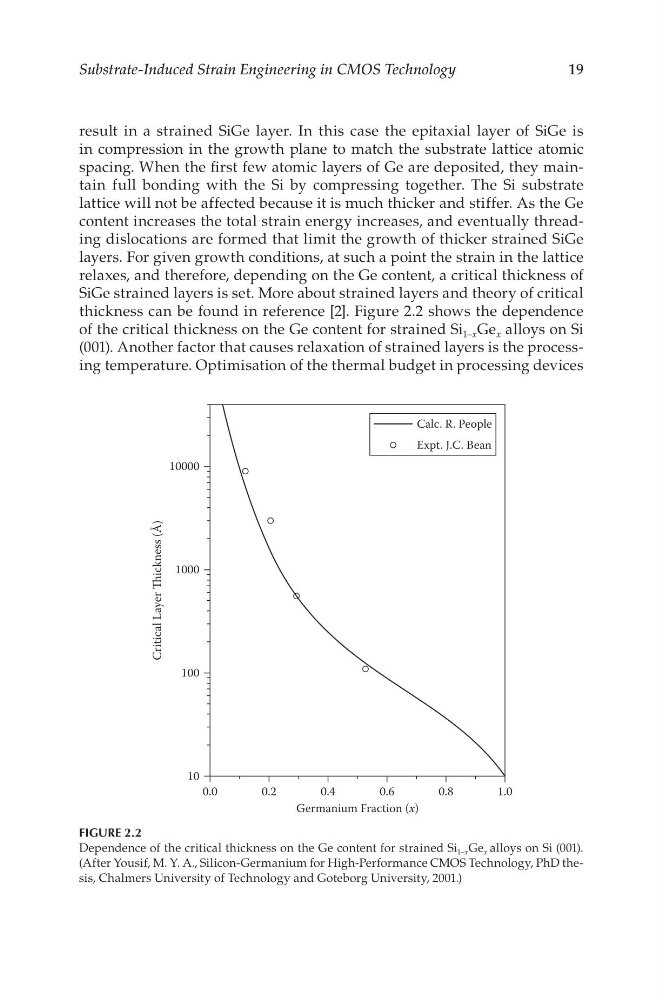
thickness can be found in reference [2]. Figure 2.2 shows the dependence
of the critical thickness on the Ge content for strained Si 1–x Ge x alloys on Si
(001). Another factor that causes relaxation of strained layers is the processing temperature. Optimisation of the thermal budget in processing devices
FIGURE 2.2
Dependence of the critical thickness on the Ge content for strained Si 1–x Ge x alloys on Si (001).
(After Yousif, M. Y. A., Silicon-Germanium for High-Performance CMOS Technology, PhD thesis, Chalmers University of Technology and Goteborg University, 2001.)
Substrate-Induced Strain Engineering in CMOS Technology
result in a strained SiGe layer. In this case the epitaxial layer of SiGe is
in compression in the growth plane to match the substrate lattice atomic
spacing. When the first few atomic layers of Ge are deposited, they maintain full bonding with the Si by compressing together. The Si substrate
lattice will not be affected because it is much thicker and stiffer. As the Ge
content increases the total strain energy increases, and eventually threading dislocations are formed that limit the growth of thicker strained SiGe
layers. For given growth conditions, at such a point the strain in the lattice
relaxes, and therefore, depending on the Ge content, a critical thickness of
SiGe strained layers is set. More about strained layers and theory of critical
thickness can be found in reference [2]. Figure 2.2 shows the dependence
of the critical thickness on the Ge content for strained Si 1–x Ge x alloys on Si
(001). Another factor that causes relaxation of strained layers is the processing temperature. Optimisation of the thermal budget in processing devices
FIGURE 2.2
Dependence of the critical thickness on the Ge content for strained Si 1–x Ge x alloys on Si (001).
(After Yousif, M. Y. A., Silicon-Germanium for High-Performance CMOS Technology, PhD thesis, Chalmers University of Technology and Goteborg University, 2001.)