

246
Strain-Engineered MOSFETs
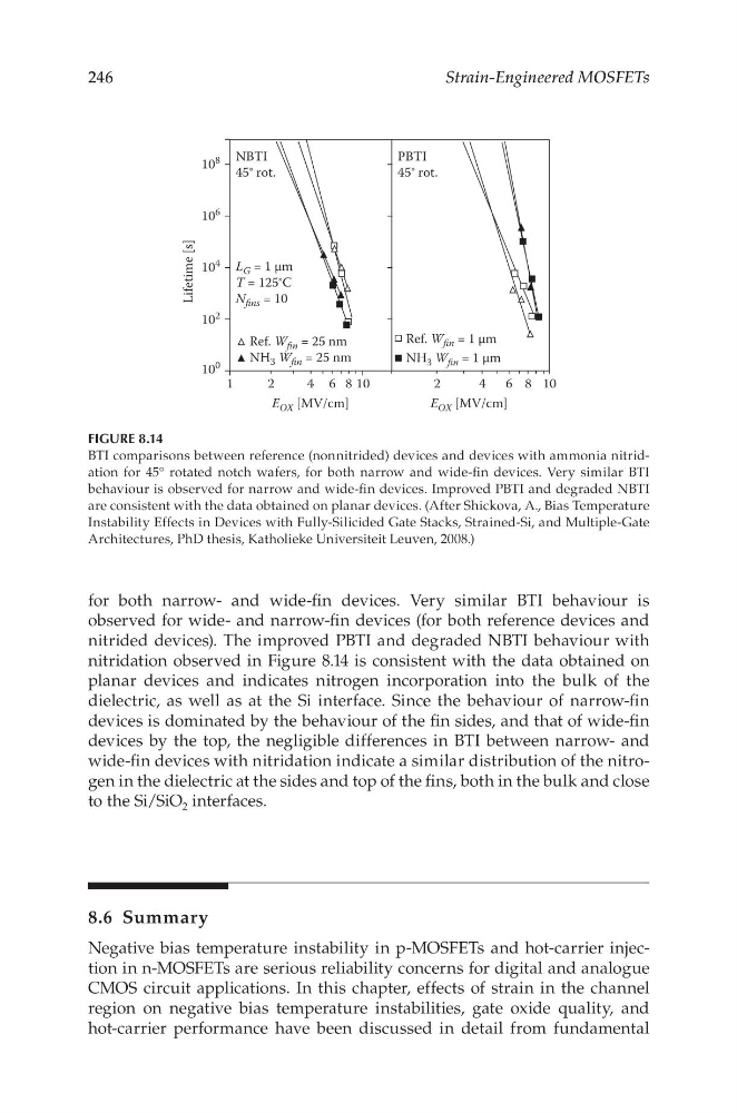
for both narrow- and wide-fin devices. Very similar BTI behaviour is
observed for wide- and narrow-fin devices (for both reference devices and
nitrided devices). The improved PBTI and degraded NBTI behaviour with
nitridation observed in Figure 8.14 is consistent with the data obtained on
planar devices and indicates nitrogen incorporation into the bulk of the
dielectric, as well as at the Si interface. Since the behaviour of narrow-fin
devices is dominated by the behaviour of the fin sides, and that of wide-fin
devices by the top, the negligible differences in BTI between narrow- and
wide-fin devices with nitridation indicate a similar distribution of the nitrogen in the dielectric at the sides and top of the fins, both in the bulk and close
to the Si/SiO 2 interfaces.
8.6 Summary
Negative bias temperature instability in p-MOSFETs and hot-carrier injection in n-MOSFETs are serious reliability concerns for digital and analogue
CMOS circuit applications. In this chapter, effects of strain in the channel
region on negative bias temperature instabilities, gate oxide quality, and
hot-carrier performance have been discussed in detail from fundamental
10
8
10
6
10
4
Lifetime [s]
10
2
10
0
1
2
4
E OX [MV/cm]
E OX [MV/cm]
Ref. W fin = 1 μm
NH 3 W fin = 1 μm
6 8 10
2
4 6 8 10
NBTI
45° rot.
PBTI
45° rot.
L G = 1 μm
T = 125°C
N fins = 10
Ref. W fin = 25 nm
NH 3 W fin = 25 nm
FIGURE 8.14
BTI comparisons between reference (nonnitrided) devices and devices with ammonia nitridation for 45° rotated notch wafers, for both narrow and wide-fin devices. Very similar BTI
behaviour is observed for narrow and wide-fin devices. Improved PBTI and degraded NBTI
are consistent with the data obtained on planar devices. (After Shickova, A., Bias Temperature
Instability Effects in Devices with Fully-Silicided Gate Stacks, Strained-Si, and Multiple-Gate
Architectures, PhD thesis, Katholieke Universiteit Leuven, 2008.)
Strain-Engineered MOSFETs
for both narrow- and wide-fin devices. Very similar BTI behaviour is
observed for wide- and narrow-fin devices (for both reference devices and
nitrided devices). The improved PBTI and degraded NBTI behaviour with
nitridation observed in Figure 8.14 is consistent with the data obtained on
planar devices and indicates nitrogen incorporation into the bulk of the
dielectric, as well as at the Si interface. Since the behaviour of narrow-fin
devices is dominated by the behaviour of the fin sides, and that of wide-fin
devices by the top, the negligible differences in BTI between narrow- and
wide-fin devices with nitridation indicate a similar distribution of the nitrogen in the dielectric at the sides and top of the fins, both in the bulk and close
to the Si/SiO 2 interfaces.
8.6 Summary
Negative bias temperature instability in p-MOSFETs and hot-carrier injection in n-MOSFETs are serious reliability concerns for digital and analogue
CMOS circuit applications. In this chapter, effects of strain in the channel
region on negative bias temperature instabilities, gate oxide quality, and
hot-carrier performance have been discussed in detail from fundamental
10
8
10
6
10
4
Lifetime [s]
10
2
10
0
1
2
4
E OX [MV/cm]
E OX [MV/cm]
Ref. W fin = 1 μm
NH 3 W fin = 1 μm
6 8 10
2
4 6 8 10
NBTI
45° rot.
PBTI
45° rot.
L G = 1 μm
T = 125°C
N fins = 10
Ref. W fin = 25 nm
NH 3 W fin = 25 nm
FIGURE 8.14
BTI comparisons between reference (nonnitrided) devices and devices with ammonia nitridation for 45° rotated notch wafers, for both narrow and wide-fin devices. Very similar BTI
behaviour is observed for narrow and wide-fin devices. Improved PBTI and degraded NBTI
are consistent with the data obtained on planar devices. (After Shickova, A., Bias Temperature
Instability Effects in Devices with Fully-Silicided Gate Stacks, Strained-Si, and Multiple-Gate
Architectures, PhD thesis, Katholieke Universiteit Leuven, 2008.)