

239
Reliability and Degradation of Strain-Engineered MOSFETs
operating conditions and the I ds -V gs sweep is performed again. Simulated
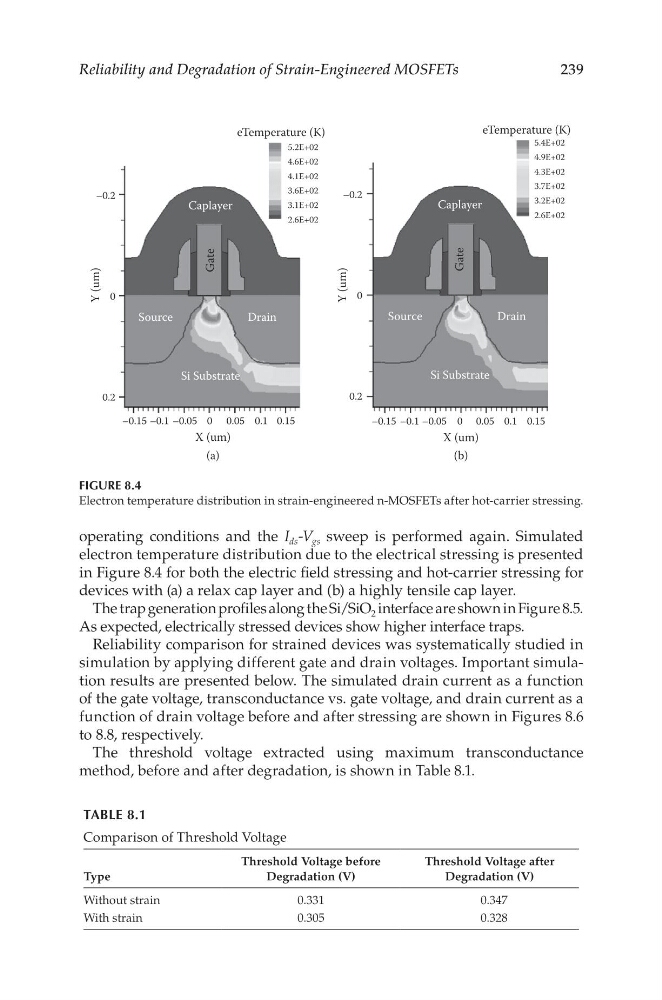
electron temperature distribution due to the electrical stressing is presented
in Figure 8.4 for both the electric field stressing and hot-carrier stressing for
devices with (a) a relax cap layer and (b) a highly tensile cap layer.
The trap generation profiles along the Si/SiO 2 interface are shown in Figure 8.5.
As expected, electrically stressed devices show higher interface traps.
Reliability comparison for strained devices was systematically studied in
simulation by applying different gate and drain voltages. Important simulation results are presented below. The simulated drain current as a function
of the gate voltage, transconductance vs. gate voltage, and drain current as a
function of drain voltage before and after stressing are shown in Figures 8.6
to 8.8, respectively.
The threshold voltage extracted using maximum transconductance
method, before and after degradation, is shown in Table 8.1.
FIGURE 8.4
Electron temperature distribution in strain-engineered n-MOSFETs after hot-carrier stressing.
TABLE 8.1
Comparison of Threshold Voltage
Type
Threshold Voltage before
Degradation (V)
Threshold Voltage after
Degradation (V)
Without strain
0.331
0.347
With strain
0.305
0.328
Reliability and Degradation of Strain-Engineered MOSFETs
operating conditions and the I ds -V gs sweep is performed again. Simulated
electron temperature distribution due to the electrical stressing is presented
in Figure 8.4 for both the electric field stressing and hot-carrier stressing for
devices with (a) a relax cap layer and (b) a highly tensile cap layer.
The trap generation profiles along the Si/SiO 2 interface are shown in Figure 8.5.
As expected, electrically stressed devices show higher interface traps.
Reliability comparison for strained devices was systematically studied in
simulation by applying different gate and drain voltages. Important simulation results are presented below. The simulated drain current as a function
of the gate voltage, transconductance vs. gate voltage, and drain current as a
function of drain voltage before and after stressing are shown in Figures 8.6
to 8.8, respectively.
The threshold voltage extracted using maximum transconductance
method, before and after degradation, is shown in Table 8.1.
FIGURE 8.4
Electron temperature distribution in strain-engineered n-MOSFETs after hot-carrier stressing.
TABLE 8.1
Comparison of Threshold Voltage
Type
Threshold Voltage before
Degradation (V)
Threshold Voltage after
Degradation (V)
Without strain
0.331
0.347
With strain
0.305
0.328