

213
Technology CAD of Strain-Engineered MOSFETs
an edge force is developed as the film grows over the spacer and gate. The
channel stress developed depends on various parameters, such as nitride
thickness, poly-thickness, spacer width, gate length, and S/D opening.
Figure 7.1(b) shows the device simulated with a highly tensile cap layer. It
shows that stresses in the cap layer lead to tensile stress in the channel area
of n-MOSFETs.
–0.6
–0.8
–1.0
–1.2
–1.4
40
60
80
100
120
140 160
Channel Stress ε
xx (GPa)
Gate Length (nm)
Recess: 40 nm
Recess: 60 nm
Recess: 80 nm
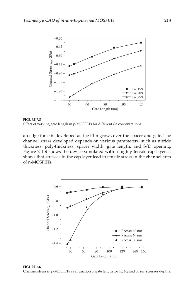
FIGURE 7.6
Channel stress in p-MOSFETs as a function of gate length for 45, 60, and 80 nm stressor depths.
–0.30
–0.45
–0.60
–0.75
–0.90
–1.05
–1.20
–1.35
40
60
80
100
120
Channel Stress ε
xx (GPa)
Gate Length (nm)
Ge 15%
Ge 20%
Ge 25%
FIGURE 7.5
Effect of varying gate length in p-MOSFETs for different Ge concentrations.
Technology CAD of Strain-Engineered MOSFETs
an edge force is developed as the film grows over the spacer and gate. The
channel stress developed depends on various parameters, such as nitride
thickness, poly-thickness, spacer width, gate length, and S/D opening.
Figure 7.1(b) shows the device simulated with a highly tensile cap layer. It
shows that stresses in the cap layer lead to tensile stress in the channel area
of n-MOSFETs.
–0.6
–0.8
–1.0
–1.2
–1.4
40
60
80
100
120
140 160
Channel Stress ε
xx (GPa)
Gate Length (nm)
Recess: 40 nm
Recess: 60 nm
Recess: 80 nm
FIGURE 7.6
Channel stress in p-MOSFETs as a function of gate length for 45, 60, and 80 nm stressor depths.
–0.30
–0.45
–0.60
–0.75
–0.90
–1.05
–1.20
–1.35
40
60
80
100
120
Channel Stress ε
xx (GPa)
Gate Length (nm)
Ge 15%
Ge 20%
Ge 25%
FIGURE 7.5
Effect of varying gate length in p-MOSFETs for different Ge concentrations.