

191
Noise in Strain-Engineered Devices
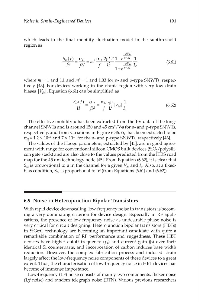
which leads to the final mobility fluctuation model in the subthreshold
region as
S f
I
fN
m f
kT
L
e
e
I
( )
2
1
1
1
Id
d
H
H
qV
m kT
qV
m kT
d
2
/
2
ds
ds
/
/
=
α =
α
µ
−
+
−
−
(6.61)
where m = 1 and 1.1 and m’ = 1 and 1.03 for n- and p-type SNWTs, respectively [43]. For devices working in the ohmic region with very low drain
biases |V ds |, Equation (6.61) can be simplified as
S f
I
fN
f
q
L
V I
( )
| |
1
id
d
H
H
ds
d
2
2
=
α =
α µ
(6.62)
The effective mobility μ has been extracted from the I-V data of the longchannel SNWTs and is around 150 and 45 cm 2 /V·s for n- and p-type SNWTs,
respectively, and from variations in Figure 6.36, α H has been extracted to be
α H ≈ 1.2 × 10 −4 and 7 × 10 −5 for the n- and p-type SNWTs, respectively [43].
The values of the Hooge parameters, extracted by [43], are in good agreement with range for conventional silicon CMOS bulk devices (SiO 2 /polysilicon gate stack) and are also close to the values predicted from the ITRS road
map for the 45 nm technology node [45]. From Equation (6.62), it is clear that
S Id is proportional to μ in the channel for a given V ds and I d . Also, at a fixedbias condition, S Id is proportional to μ 2 (from Equations (6.61) and (6.62)).
6.9 Noise in Heterojunction Bipolar Transistors
With rapid device downscaling, low-frequency noise in transistors is becoming a very dominating criterion for device design. Especially in RF applications, the presence of low-frequency noise as undesirable phase noise is
very critical for circuit designing. Heterojunction bipolar transistors (HBTs)
in SiGe:C technology are becoming an important candidate with quite a
remarkable combination of RF performance and ruggedness. These HBT
devices have higher cutoff frequency (f T ) and current gain (β) over their
identical Si counterparts, and incorporation of carbon induces base width
reduction. However, the complex fabrication process and induced strain
largely affect the low-frequency noise components of these devices to a great
extent. Thus, the characterisation of low-frequency noise in HBT devices has
become of immense importance.
Low-frequency (LF) noise consists of mainly two components, flicker noise
(1/f noise) and random telegraph noise (RTN). Various previous researchers
Noise in Strain-Engineered Devices
which leads to the final mobility fluctuation model in the subthreshold
region as
S f
I
fN
m f
kT
L
e
e
I
( )
2
1
1
1
Id
d
H
H
qV
m kT
qV
m kT
d
2
/
2
ds
ds
/
/
=
α =
α
µ
−
+
−
−
(6.61)
where m = 1 and 1.1 and m’ = 1 and 1.03 for n- and p-type SNWTs, respectively [43]. For devices working in the ohmic region with very low drain
biases |V ds |, Equation (6.61) can be simplified as
S f
I
fN
f
q
L
V I
( )
| |
1
id
d
H
H
ds
d
2
2
=
α =
α µ
(6.62)
The effective mobility μ has been extracted from the I-V data of the longchannel SNWTs and is around 150 and 45 cm 2 /V·s for n- and p-type SNWTs,
respectively, and from variations in Figure 6.36, α H has been extracted to be
α H ≈ 1.2 × 10 −4 and 7 × 10 −5 for the n- and p-type SNWTs, respectively [43].
The values of the Hooge parameters, extracted by [43], are in good agreement with range for conventional silicon CMOS bulk devices (SiO 2 /polysilicon gate stack) and are also close to the values predicted from the ITRS road
map for the 45 nm technology node [45]. From Equation (6.62), it is clear that
S Id is proportional to μ in the channel for a given V ds and I d . Also, at a fixedbias condition, S Id is proportional to μ 2 (from Equations (6.61) and (6.62)).
6.9 Noise in Heterojunction Bipolar Transistors
With rapid device downscaling, low-frequency noise in transistors is becoming a very dominating criterion for device design. Especially in RF applications, the presence of low-frequency noise as undesirable phase noise is
very critical for circuit designing. Heterojunction bipolar transistors (HBTs)
in SiGe:C technology are becoming an important candidate with quite a
remarkable combination of RF performance and ruggedness. These HBT
devices have higher cutoff frequency (f T ) and current gain (β) over their
identical Si counterparts, and incorporation of carbon induces base width
reduction. However, the complex fabrication process and induced strain
largely affect the low-frequency noise components of these devices to a great
extent. Thus, the characterisation of low-frequency noise in HBT devices has
become of immense importance.
Low-frequency (LF) noise consists of mainly two components, flicker noise
(1/f noise) and random telegraph noise (RTN). Various previous researchers