

188
Strain-Engineered MOSFETs
due to the small size of the NW channel, adds complexities to the extraction
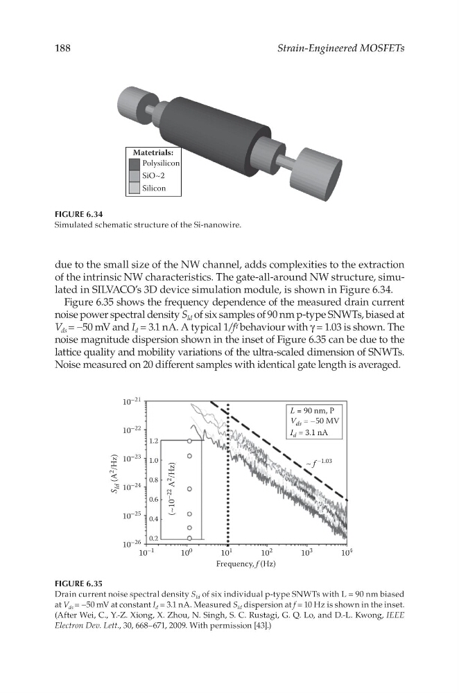
of the intrinsic NW characteristics. The gate-all-around NW structure, simulated in SILVACO’s 3D device simulation module, is shown in Figure 6.34.
Figure 6.35 shows the frequency dependence of the measured drain current
noise power spectral density S Id of six samples of 90 nm p-type SNWTs, biased at
V ds = −50 mV and I d = 3.1 nA. A typical 1/f γ behaviour with γ = 1.03 is shown. The
noise magnitude dispersion shown in the inset of Figure 6.35 can be due to the
lattice quality and mobility variations of the ultra-scaled dimension of SNWTs.
Noise measured on 20 different samples with identical gate length is averaged.
Matetrials:
Polysilicon
SiO~2
Silicon
FIGURE 6.34
Simulated schematic structure of the Si-nanowire.
10
–1
10
–26
10
–25
10
–24
(~10
–22
A
2
/Hz)
10
–23
1.2
1.0
L = 90 nm, P
V ds = –50 MV
I d = 3.1 nA
0.8
0.6
0.4
0.2
10
–22
S
Id (A
2
/Hz)
10
–21
10
0
10
1
~ f
–1.03
Frequency, f (Hz)
10
2
10
3
10
4
FIGURE 6.35
Drain current noise spectral density S Id of six individual p-type SNWTs with L = 90 nm biased
at V ds = −50 mV at constant I d = 3.1 nA. Measured S Id dispersion at f = 10 Hz is shown in the inset.
(After Wei, C., Y.-Z. Xiong, X. Zhou, N. Singh, S. C. Rustagi, G. Q. Lo, and D.-L. Kwong, IEEE
Electron Dev. Lett., 30, 668–671, 2009. With permission [43].)
Strain-Engineered MOSFETs
due to the small size of the NW channel, adds complexities to the extraction
of the intrinsic NW characteristics. The gate-all-around NW structure, simulated in SILVACO’s 3D device simulation module, is shown in Figure 6.34.
Figure 6.35 shows the frequency dependence of the measured drain current
noise power spectral density S Id of six samples of 90 nm p-type SNWTs, biased at
V ds = −50 mV and I d = 3.1 nA. A typical 1/f γ behaviour with γ = 1.03 is shown. The
noise magnitude dispersion shown in the inset of Figure 6.35 can be due to the
lattice quality and mobility variations of the ultra-scaled dimension of SNWTs.
Noise measured on 20 different samples with identical gate length is averaged.
Matetrials:
Polysilicon
SiO~2
Silicon
FIGURE 6.34
Simulated schematic structure of the Si-nanowire.
10
–1
10
–26
10
–25
10
–24
(~10
–22
A
2
/Hz)
10
–23
1.2
1.0
L = 90 nm, P
V ds = –50 MV
I d = 3.1 nA
0.8
0.6
0.4
0.2
10
–22
S
Id (A
2
/Hz)
10
–21
10
0
10
1
~ f
–1.03
Frequency, f (Hz)
10
2
10
3
10
4
FIGURE 6.35
Drain current noise spectral density S Id of six individual p-type SNWTs with L = 90 nm biased
at V ds = −50 mV at constant I d = 3.1 nA. Measured S Id dispersion at f = 10 Hz is shown in the inset.
(After Wei, C., Y.-Z. Xiong, X. Zhou, N. Singh, S. C. Rustagi, G. Q. Lo, and D.-L. Kwong, IEEE
Electron Dev. Lett., 30, 668–671, 2009. With permission [43].)