

179
Noise in Strain-Engineered Devices
where Q s represents the area charge density of the conducting carriers in the
channel. Equation (6.53) shows that the drain current noise power density is
proportional to W/L 3 , as observed in our results. From Equation (6.53), it can
be deduced that even if one scales down W and L by the same proportion
such that the W/L ratio remains constant, the drain current noise would still
increase by 1/L 2 with technology downscaling. This raises a concern about
the 1/f noise performance of future generations of ultra-deep submicrometer
MOSFETs, where low drain current noise is desired.
It is known that the 1/f noises of n-MOS and p-MOS transistors tend to
show different gate voltage dependencies [39]. There are two existing explanations for these differences. The first one says the noises of n-MOS and p-MOS
transistors are two different mechanisms: surface trapping mechanism for
n-MOS transistors and bulk mobility fluctuation mechanism (Hooge’s model)
for p-MOS transistors. The second one says the noises of both n-MOS and
p-MOS transistors are due to trapping, with the trap density constant for
n-MOS transistors and varying with gate voltage for p-MOS transistors [39].
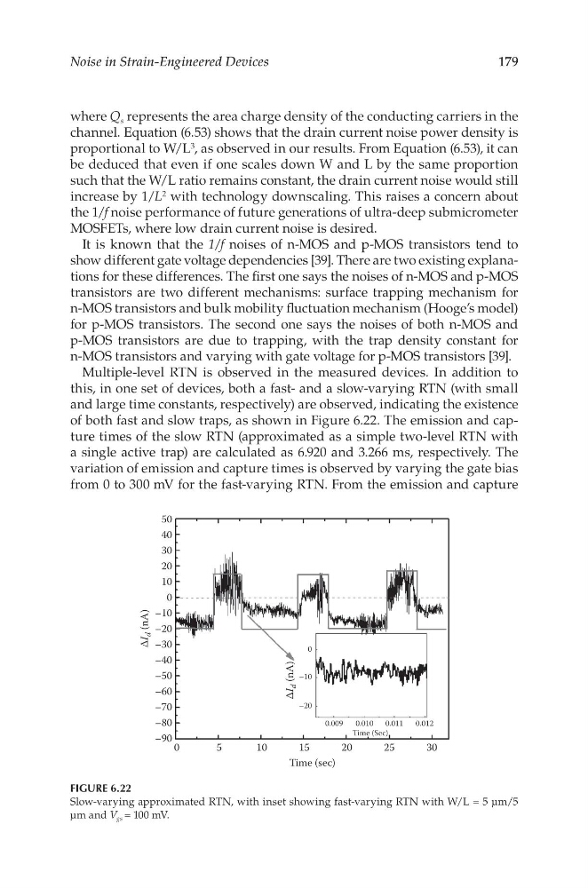
Multiple-level RTN is observed in the measured devices. In addition to
this, in one set of devices, both a fast- and a slow-varying RTN (with small
and large time constants, respectively) are observed, indicating the existence
of both fast and slow traps, as shown in Figure 6.22. The emission and capture times of the slow RTN (approximated as a simple two-level RTN with
a single active trap) are calculated as 6.920 and 3.266 ms, respectively. The
variation of emission and capture times is observed by varying the gate bias
from 0 to 300 mV for the fast-varying RTN. From the emission and capture
Time (sec)
0
–90
–80
–70
–60
–50
–40
–30
–20
∆I
d (nA)
∆I
d (nA)
–10
0
0
–10
0.009
0.010
Time (Sec)
0.011
0.012
–20
10
20
30
40
50
5
1 0
1 5
2 0
2 5
3 0
FIGURE 6.22
Slow-varying approximated RTN, with inset showing fast-varying RTN with W/L = 5 μm/5
μm and V gs = 100 mV.
Noise in Strain-Engineered Devices
where Q s represents the area charge density of the conducting carriers in the
channel. Equation (6.53) shows that the drain current noise power density is
proportional to W/L 3 , as observed in our results. From Equation (6.53), it can
be deduced that even if one scales down W and L by the same proportion
such that the W/L ratio remains constant, the drain current noise would still
increase by 1/L 2 with technology downscaling. This raises a concern about
the 1/f noise performance of future generations of ultra-deep submicrometer
MOSFETs, where low drain current noise is desired.
It is known that the 1/f noises of n-MOS and p-MOS transistors tend to
show different gate voltage dependencies [39]. There are two existing explanations for these differences. The first one says the noises of n-MOS and p-MOS
transistors are two different mechanisms: surface trapping mechanism for
n-MOS transistors and bulk mobility fluctuation mechanism (Hooge’s model)
for p-MOS transistors. The second one says the noises of both n-MOS and
p-MOS transistors are due to trapping, with the trap density constant for
n-MOS transistors and varying with gate voltage for p-MOS transistors [39].
Multiple-level RTN is observed in the measured devices. In addition to
this, in one set of devices, both a fast- and a slow-varying RTN (with small
and large time constants, respectively) are observed, indicating the existence
of both fast and slow traps, as shown in Figure 6.22. The emission and capture times of the slow RTN (approximated as a simple two-level RTN with
a single active trap) are calculated as 6.920 and 3.266 ms, respectively. The
variation of emission and capture times is observed by varying the gate bias
from 0 to 300 mV for the fast-varying RTN. From the emission and capture
Time (sec)
0
–90
–80
–70
–60
–50
–40
–30
–20
∆I
d (nA)
∆I
d (nA)
–10
0
0
–10
0.009
0.010
Time (Sec)
0.011
0.012
–20
10
20
30
40
50
5
1 0
1 5
2 0
2 5
3 0
FIGURE 6.22
Slow-varying approximated RTN, with inset showing fast-varying RTN with W/L = 5 μm/5
μm and V gs = 100 mV.