

163
Noise in Strain-Engineered Devices
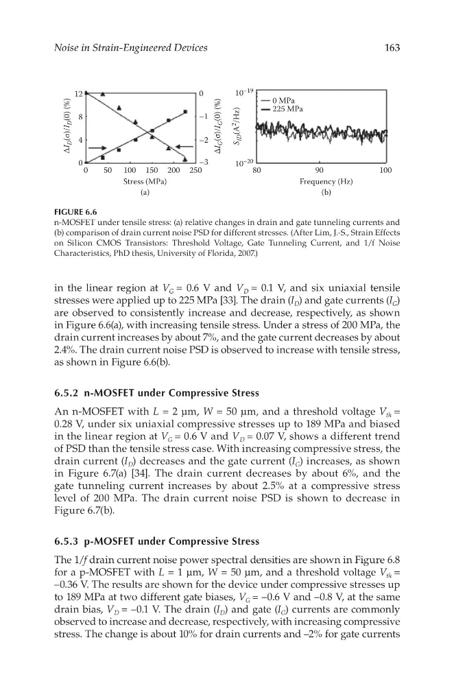
in the linear region at V G = 0.6 V and V D = 0.1 V, and six uniaxial tensile
stresses were applied up to 225 MPa [33]. The drain (I D ) and gate currents (I G )
are observed to consistently increase and decrease, respectively, as shown
in Figure 6.6(a), with increasing tensile stress. Under a stress of 200 MPa, the
drain current increases by about 7%, and the gate current decreases by about
2.4%. The drain current noise PSD is observed to increase with tensile stress,
as shown in Figure 6.6(b).
6.5.2 n-MOSFET under Compressive Stress
An n-MOSFET with L = 2 μm, W = 50 μm, and a threshold voltage V th =
0.28 V, under six uniaxial compressive stresses up to 189 MPa and biased
in the linear region at V G = 0.6 V and V D = 0.07 V, shows a different trend
of PSD than the tensile stress case. With increasing compressive stress, the
drain current (I D ) decreases and the gate current (I G ) increases, as shown
in Figure 6.7(a) [34]. The drain current decreases by about 6%, and the
gate tunneling current increases by about 2.5% at a compressive stress
level of 200 MPa. The drain current noise PSD is shown to decrease in
Figure 6.7(b).
6.5.3 p-MOSFET under Compressive Stress
The 1/f drain current noise power spectral densities are shown in Figure 6.8
for a p-MOSFET with L = 1 μm, W = 50 μm, and a threshold voltage V th =
–0.36 V. The results are shown for the device under compressive stresses up
to 189 MPa at two different gate biases, V G = –0.6 V and –0.8 V, at the same
drain bias, V D = –0.1 V. The drain (I D ) and gate (I G ) currents are commonly
observed to increase and decrease, respectively, with increasing compressive
stress. The change is about 10% for drain currents and –2% for gate currents
12
10
–19
10
–20
8
–1
0
0 MPa
225 MPa
–2
–3
∆I
D (σ)/I
D (0) (%)
∆I
G (σ)/I
G (0) (%)
S
ID (A
2
/Hz)
4
0 0
50 100
Stress (MPa)
Frequency (Hz)
(a)
(b)
150 200 250
80
90
100
FIGURE 6.6
n-MOSFET under tensile stress: (a) relative changes in drain and gate tunneling currents and
(b) comparison of drain current noise PSD for different stresses. (After Lim, J.-S., Strain Effects
on Silicon CMOS Transistors: Threshold Voltage, Gate Tunneling Current, and 1/f Noise
Characteristics, PhD thesis, University of Florida, 2007.)
Noise in Strain-Engineered Devices
in the linear region at V G = 0.6 V and V D = 0.1 V, and six uniaxial tensile
stresses were applied up to 225 MPa [33]. The drain (I D ) and gate currents (I G )
are observed to consistently increase and decrease, respectively, as shown
in Figure 6.6(a), with increasing tensile stress. Under a stress of 200 MPa, the
drain current increases by about 7%, and the gate current decreases by about
2.4%. The drain current noise PSD is observed to increase with tensile stress,
as shown in Figure 6.6(b).
6.5.2 n-MOSFET under Compressive Stress
An n-MOSFET with L = 2 μm, W = 50 μm, and a threshold voltage V th =
0.28 V, under six uniaxial compressive stresses up to 189 MPa and biased
in the linear region at V G = 0.6 V and V D = 0.07 V, shows a different trend
of PSD than the tensile stress case. With increasing compressive stress, the
drain current (I D ) decreases and the gate current (I G ) increases, as shown
in Figure 6.7(a) [34]. The drain current decreases by about 6%, and the
gate tunneling current increases by about 2.5% at a compressive stress
level of 200 MPa. The drain current noise PSD is shown to decrease in
Figure 6.7(b).
6.5.3 p-MOSFET under Compressive Stress
The 1/f drain current noise power spectral densities are shown in Figure 6.8
for a p-MOSFET with L = 1 μm, W = 50 μm, and a threshold voltage V th =
–0.36 V. The results are shown for the device under compressive stresses up
to 189 MPa at two different gate biases, V G = –0.6 V and –0.8 V, at the same
drain bias, V D = –0.1 V. The drain (I D ) and gate (I G ) currents are commonly
observed to increase and decrease, respectively, with increasing compressive
stress. The change is about 10% for drain currents and –2% for gate currents
12
10
–19
10
–20
8
–1
0
0 MPa
225 MPa
–2
–3
∆I
D (σ)/I
D (0) (%)
∆I
G (σ)/I
G (0) (%)
S
ID (A
2
/Hz)
4
0 0
50 100
Stress (MPa)
Frequency (Hz)
(a)
(b)
150 200 250
80
90
100
FIGURE 6.6
n-MOSFET under tensile stress: (a) relative changes in drain and gate tunneling currents and
(b) comparison of drain current noise PSD for different stresses. (After Lim, J.-S., Strain Effects
on Silicon CMOS Transistors: Threshold Voltage, Gate Tunneling Current, and 1/f Noise
Characteristics, PhD thesis, University of Florida, 2007.)