

162
Strain-Engineered MOSFETs
identified as the occupied state of the trap, the traps can be identified as
acceptor traps. Thus the high current time was considered as τ e and the low
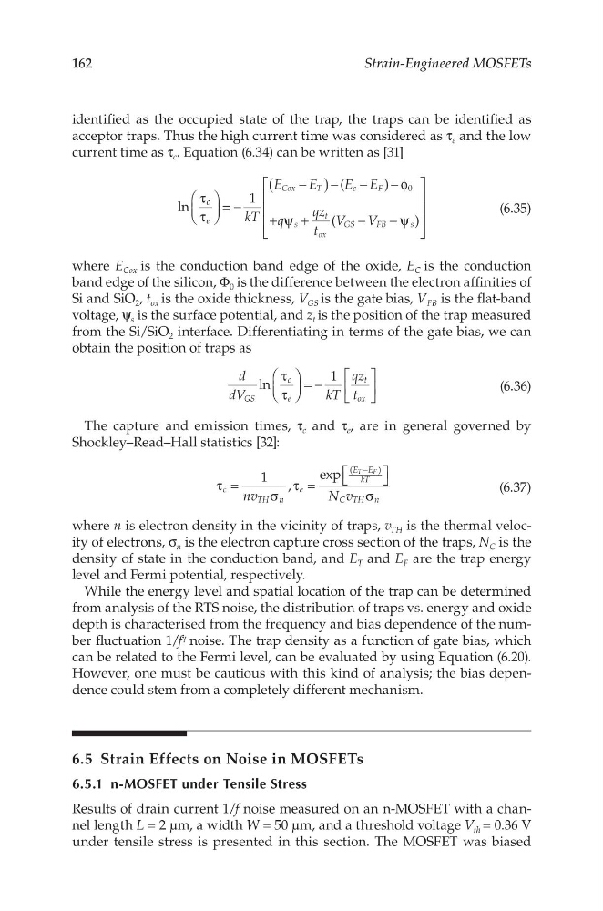
current time as τ c . Equation (6.34) can be written as [31]
kT
E
E
E E
q
qz
t
V
V
ln
1
(
)
(
)
c
e
Cox
T
c
F
s
t
ox
GS
FB
s
0
(
)
τ
τ
= −
−
−
−
−φ
+ ψ +
−
− ψ
(6.35)
where E Cox is the conduction band edge of the oxide, E C is the conduction
band edge of the silicon, Φ 0 is the difference between the electron affinities of
Si and SiO 2 , t ox is the oxide thickness, V GS is the gate bias, V FB is the flat-band
voltage, ψ s is the surface potential, and z t is the position of the trap measured
from the Si/SiO 2 interface. Differentiating in terms of the gate bias, we can
obtain the position of traps as
d
dV
kT
qz
t
ln
1
GS
c
e
t
ox
τ
τ
= −
(6.36)
The capture and emission times, τ c and τ e , are in general governed by
Shockley–Read–Hall statistics [32]:
nv
N v
1 ,
exp
c
TH n
e
E E
kT
C TH n
(
)
T
F
τ =
σ
τ =
σ
−
(6.37)
where n is electron density in the vicinity of traps, v TH is the thermal velocity of electrons, σ n is the electron capture cross section of the traps, N C is the
density of state in the conduction band, and E T and E F are the trap energy
level and Fermi potential, respectively.
While the energy level and spatial location of the trap can be determined
from analysis of the RTS noise, the distribution of traps vs. energy and oxide
depth is characterised from the frequency and bias dependence of the number fluctuation 1/f γ noise. The trap density as a function of gate bias, which
can be related to the Fermi level, can be evaluated by using Equation (6.20).
However, one must be cautious with this kind of analysis; the bias dependence could stem from a completely different mechanism.
6.5 Strain Effects on Noise in MOSFETs
6.5.1 n-MOSFET under Tensile Stress
Results of drain current 1/f noise measured on an n-MOSFET with a channel length L = 2 μm, a width W = 50 μm, and a threshold voltage V th = 0.36 V
under tensile stress is presented in this section. The MOSFET was biased
Strain-Engineered MOSFETs
identified as the occupied state of the trap, the traps can be identified as
acceptor traps. Thus the high current time was considered as τ e and the low
current time as τ c . Equation (6.34) can be written as [31]
kT
E
E
E E
q
qz
t
V
V
ln
1
(
)
(
)
c
e
Cox
T
c
F
s
t
ox
GS
FB
s
0
(
)
τ
τ
= −
−
−
−
−φ
+ ψ +
−
− ψ
(6.35)
where E Cox is the conduction band edge of the oxide, E C is the conduction
band edge of the silicon, Φ 0 is the difference between the electron affinities of
Si and SiO 2 , t ox is the oxide thickness, V GS is the gate bias, V FB is the flat-band
voltage, ψ s is the surface potential, and z t is the position of the trap measured
from the Si/SiO 2 interface. Differentiating in terms of the gate bias, we can
obtain the position of traps as
d
dV
kT
qz
t
ln
1
GS
c
e
t
ox
τ
τ
= −
(6.36)
The capture and emission times, τ c and τ e , are in general governed by
Shockley–Read–Hall statistics [32]:
nv
N v
1 ,
exp
c
TH n
e
E E
kT
C TH n
(
)
T
F
τ =
σ
τ =
σ
−
(6.37)
where n is electron density in the vicinity of traps, v TH is the thermal velocity of electrons, σ n is the electron capture cross section of the traps, N C is the
density of state in the conduction band, and E T and E F are the trap energy
level and Fermi potential, respectively.
While the energy level and spatial location of the trap can be determined
from analysis of the RTS noise, the distribution of traps vs. energy and oxide
depth is characterised from the frequency and bias dependence of the number fluctuation 1/f γ noise. The trap density as a function of gate bias, which
can be related to the Fermi level, can be evaluated by using Equation (6.20).
However, one must be cautious with this kind of analysis; the bias dependence could stem from a completely different mechanism.
6.5 Strain Effects on Noise in MOSFETs
6.5.1 n-MOSFET under Tensile Stress
Results of drain current 1/f noise measured on an n-MOSFET with a channel length L = 2 μm, a width W = 50 μm, and a threshold voltage V th = 0.36 V
under tensile stress is presented in this section. The MOSFET was biased