

159
Noise in Strain-Engineered Devices
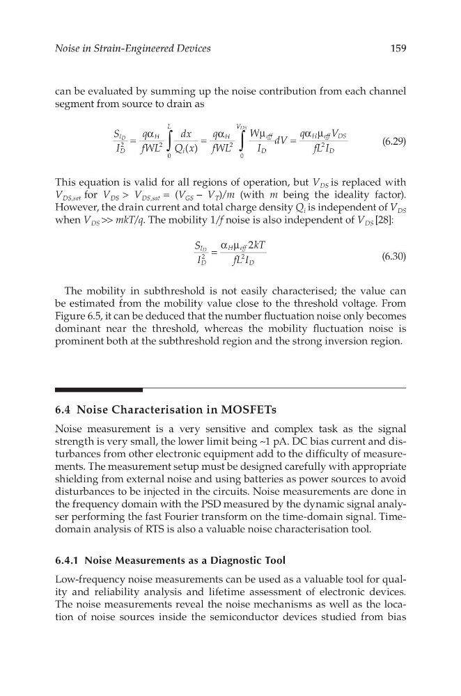
can be evaluated by summing up the noise contribution from each channel
segment from source to drain as
S
I
q
fWL
dx
Q x
q
fWL
W
I
dV
q
V
fL I
( )
I
D
H
i
L
H
eff
D
V
H eff DS
D
2
2
0
2
0
2
D
DS
∫
∫
=
α
=
α
µ
=
α µ
(6.29)
This equation is valid for all regions of operation, but V DS is replaced with
V DS,sat for V DS > V DS,sat = (V GS – V T )/m (with m being the ideality factor).
However, the drain current and total charge density Q i is independent of V DS
when V DS >> mkT/q. The mobility 1/f noise is also independent of V DS [28]:
S
I
kT
fL I
2
I
D
H eff
D
2
2
D
=
α µ
(6.30)
The mobility in subthreshold is not easily characterised; the value can
be estimated from the mobility value close to the threshold voltage. From
Figure 6.5, it can be deduced that the number fluctuation noise only becomes
dominant near the threshold, whereas the mobility fluctuation noise is
prominent both at the subthreshold region and the strong inversion region.
6.4 Noise Characterisation in MOSFETs
Noise measurement is a very sensitive and complex task as the signal
strength is very small, the lower limit being ~1 pA. DC bias current and disturbances from other electronic equipment add to the difficulty of measurements. The measurement setup must be designed carefully with appropriate
shielding from external noise and using batteries as power sources to avoid
disturbances to be injected in the circuits. Noise measurements are done in
the frequency domain with the PSD measured by the dynamic signal analyser performing the fast Fourier transform on the time-domain signal. Timedomain analysis of RTS is also a valuable noise characterisation tool.
6.4.1 Noise Measurements as a Diagnostic Tool
Low-frequency noise measurements can be used as a valuable tool for quality and reliability analysis and lifetime assessment of electronic devices.
The noise measurements reveal the noise mechanisms as well as the location of noise sources inside the semiconductor devices studied from bias
Noise in Strain-Engineered Devices
can be evaluated by summing up the noise contribution from each channel
segment from source to drain as
S
I
q
fWL
dx
Q x
q
fWL
W
I
dV
q
V
fL I
( )
I
D
H
i
L
H
eff
D
V
H eff DS
D
2
2
0
2
0
2
D
DS
∫
∫
=
α
=
α
µ
=
α µ
(6.29)
This equation is valid for all regions of operation, but V DS is replaced with
V DS,sat for V DS > V DS,sat = (V GS – V T )/m (with m being the ideality factor).
However, the drain current and total charge density Q i is independent of V DS
when V DS >> mkT/q. The mobility 1/f noise is also independent of V DS [28]:
S
I
kT
fL I
2
I
D
H eff
D
2
2
D
=
α µ
(6.30)
The mobility in subthreshold is not easily characterised; the value can
be estimated from the mobility value close to the threshold voltage. From
Figure 6.5, it can be deduced that the number fluctuation noise only becomes
dominant near the threshold, whereas the mobility fluctuation noise is
prominent both at the subthreshold region and the strong inversion region.
6.4 Noise Characterisation in MOSFETs
Noise measurement is a very sensitive and complex task as the signal
strength is very small, the lower limit being ~1 pA. DC bias current and disturbances from other electronic equipment add to the difficulty of measurements. The measurement setup must be designed carefully with appropriate
shielding from external noise and using batteries as power sources to avoid
disturbances to be injected in the circuits. Noise measurements are done in
the frequency domain with the PSD measured by the dynamic signal analyser performing the fast Fourier transform on the time-domain signal. Timedomain analysis of RTS is also a valuable noise characterisation tool.
6.4.1 Noise Measurements as a Diagnostic Tool
Low-frequency noise measurements can be used as a valuable tool for quality and reliability analysis and lifetime assessment of electronic devices.
The noise measurements reveal the noise mechanisms as well as the location of noise sources inside the semiconductor devices studied from bias