

157
Noise in Strain-Engineered Devices
oxide charge density is greater than the change in inversion charge density as the charge trapped in the oxide is not only supplied from the inversion charge but also from the depletion and interface trap charges. The
normalised drain current noise in the subthreshold region can be written
as [25]
S
I
q N
kTf WL C
C C
(
)
I
D
t
ox
d
i t
2
4
2
D
=
λ
+ +
γ
(6.24)
where C ox , C d , and C it are the oxide, depletion capacitance, and capacitance
due to interface trapped charge.
A trap density that increases toward the conduction or valence band edges
results in a faster fall-off of S ID /I D
2 than 1/Q i
2 due to the band bending, resulting in a faster change in the oxide trap energy compared to the interface
traps. In this case γ is greater than 1 and increases with gate bias. Studies on
RTS noise in MOSFETs show that thermally activated phonon-assisted capture and emission of carriers play an important role [8]. If the time constant
of the trap is written as
e
th
th
E kT
0,
/
τ = τ
(6.25)
S
ID /I
D
2
(a.u.)
10
–8
10
–7
Eq. (6.20)
Eqs. (6.29) & (6.30)
Eqs. (6.26) & (6.30)
10
–6
Drain Current (A)
Mobility fluct.
Number fluct.
V T
10
–5
10
–4
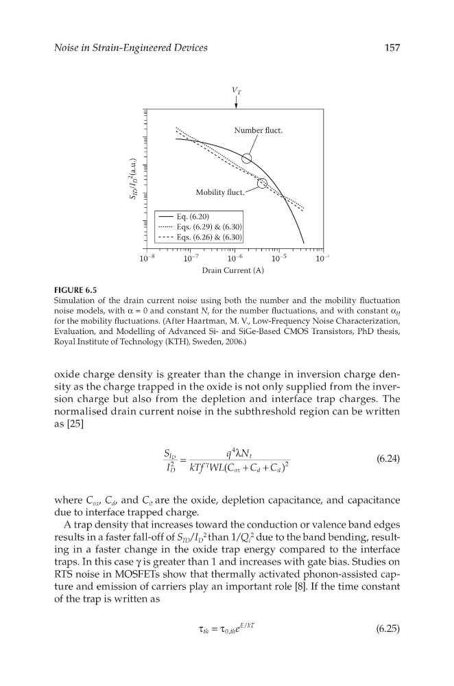
FIGURE 6.5
Simulation of the drain current noise using both the number and the mobility fluctuation
noise models, with α = 0 and constant N t for the number fluctuations, and with constant α H
for the mobility fluctuations. (After Haartman, M. V., Low-Frequency Noise Characterization,
Evaluation, and Modelling of Advanced Si- and SiGe-Based CMOS Transistors, PhD thesis,
Royal Institute of Technology (KTH), Sweden, 2006.)
Noise in Strain-Engineered Devices
oxide charge density is greater than the change in inversion charge density as the charge trapped in the oxide is not only supplied from the inversion charge but also from the depletion and interface trap charges. The
normalised drain current noise in the subthreshold region can be written
as [25]
S
I
q N
kTf WL C
C C
(
)
I
D
t
ox
d
i t
2
4
2
D
=
λ
+ +
γ
(6.24)
where C ox , C d , and C it are the oxide, depletion capacitance, and capacitance
due to interface trapped charge.
A trap density that increases toward the conduction or valence band edges
results in a faster fall-off of S ID /I D
2 than 1/Q i
2 due to the band bending, resulting in a faster change in the oxide trap energy compared to the interface
traps. In this case γ is greater than 1 and increases with gate bias. Studies on
RTS noise in MOSFETs show that thermally activated phonon-assisted capture and emission of carriers play an important role [8]. If the time constant
of the trap is written as
e
th
th
E kT
0,
/
τ = τ
(6.25)
S
ID /I
D
2
(a.u.)
10
–8
10
–7
Eq. (6.20)
Eqs. (6.29) & (6.30)
Eqs. (6.26) & (6.30)
10
–6
Drain Current (A)
Mobility fluct.
Number fluct.
V T
10
–5
10
–4
FIGURE 6.5
Simulation of the drain current noise using both the number and the mobility fluctuation
noise models, with α = 0 and constant N t for the number fluctuations, and with constant α H
for the mobility fluctuations. (After Haartman, M. V., Low-Frequency Noise Characterization,
Evaluation, and Modelling of Advanced Si- and SiGe-Based CMOS Transistors, PhD thesis,
Royal Institute of Technology (KTH), Sweden, 2006.)