

150
Strain-Engineered MOSFETs
trapped in a single trap or localised defect state, the current or voltage signal
displays a random shift in the level denoting a change in the channel resistance. In bipolar transistors, however, the trapping/de-trapping process has
different mechanisms, which will be discussed later in the chapter, involving the tunneling of carriers across the p-n junction potential barrier. The
two-level RTS signal signifies only one active trap. However, when multiple
traps are involved, the current (or voltage) can switch between two or more
states resembling a RTS waveform due to random trapping and de-trapping
of carriers, and the phenomenon is much more difficult to explain in order to
identify the trapping/de-trapping process. For simple two-level RTS pulses
with equal height ΔI and Poisson distributed mean time durations in the
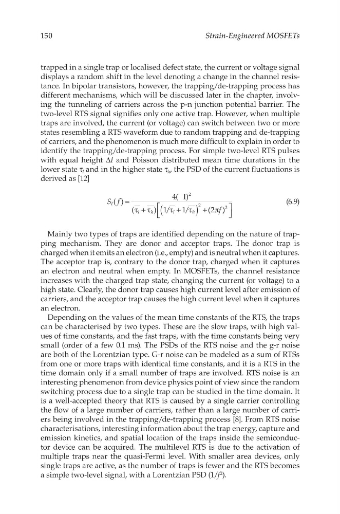
lower state τ l and in the higher state τ h , the PSD of the current fluctuations is
derived as [12]
S f
f
( )
4( )
(
) 1/
1/
(2 )
I
l
h
l
h
2
2
2
(
)
=
Ι
τ + τ
τ + τ + π
(6.9)
Mainly two types of traps are identified depending on the nature of trapping mechanism. They are donor and acceptor traps. The donor trap is
charged when it emits an electron (i.e., empty) and is neutral when it captures.
The acceptor trap is, contrary to the donor trap, charged when it captures
an electron and neutral when empty. In MOSFETs, the channel resistance
increases with the charged trap state, changing the current (or voltage) to a
high state. Clearly, the donor trap causes high current level after emission of
carriers, and the acceptor trap causes the high current level when it captures
an electron.
Depending on the values of the mean time constants of the RTS, the traps
can be characterised by two types. These are the slow traps, with high values of time constants, and the fast traps, with the time constants being very
small (order of a few 0.1 ms). The PSDs of the RTS noise and the g-r noise
are both of the Lorentzian type. G-r noise can be modeled as a sum of RTSs
from one or more traps with identical time constants, and it is a RTS in the
time domain only if a small number of traps are involved. RTS noise is an
interesting phenomenon from device physics point of view since the random
switching process due to a single trap can be studied in the time domain. It
is a well-accepted theory that RTS is caused by a single carrier controlling
the flow of a large number of carriers, rather than a large number of carriers being involved in the trapping/de-trapping process [8]. From RTS noise
characterisations, interesting information about the trap energy, capture and
emission kinetics, and spatial location of the traps inside the semiconductor device can be acquired. The multilevel RTS is due to the activation of
multiple traps near the quasi-Fermi level. With smaller area devices, only
single traps are active, as the number of traps is fewer and the RTS becomes
a simple two-level signal, with a Lorentzian PSD (1/f 2 ).
Strain-Engineered MOSFETs
trapped in a single trap or localised defect state, the current or voltage signal
displays a random shift in the level denoting a change in the channel resistance. In bipolar transistors, however, the trapping/de-trapping process has
different mechanisms, which will be discussed later in the chapter, involving the tunneling of carriers across the p-n junction potential barrier. The
two-level RTS signal signifies only one active trap. However, when multiple
traps are involved, the current (or voltage) can switch between two or more
states resembling a RTS waveform due to random trapping and de-trapping
of carriers, and the phenomenon is much more difficult to explain in order to
identify the trapping/de-trapping process. For simple two-level RTS pulses
with equal height ΔI and Poisson distributed mean time durations in the
lower state τ l and in the higher state τ h , the PSD of the current fluctuations is
derived as [12]
S f
f
( )
4( )
(
) 1/
1/
(2 )
I
l
h
l
h
2
2
2
(
)
=
Ι
τ + τ
τ + τ + π
(6.9)
Mainly two types of traps are identified depending on the nature of trapping mechanism. They are donor and acceptor traps. The donor trap is
charged when it emits an electron (i.e., empty) and is neutral when it captures.
The acceptor trap is, contrary to the donor trap, charged when it captures
an electron and neutral when empty. In MOSFETs, the channel resistance
increases with the charged trap state, changing the current (or voltage) to a
high state. Clearly, the donor trap causes high current level after emission of
carriers, and the acceptor trap causes the high current level when it captures
an electron.
Depending on the values of the mean time constants of the RTS, the traps
can be characterised by two types. These are the slow traps, with high values of time constants, and the fast traps, with the time constants being very
small (order of a few 0.1 ms). The PSDs of the RTS noise and the g-r noise
are both of the Lorentzian type. G-r noise can be modeled as a sum of RTSs
from one or more traps with identical time constants, and it is a RTS in the
time domain only if a small number of traps are involved. RTS noise is an
interesting phenomenon from device physics point of view since the random
switching process due to a single trap can be studied in the time domain. It
is a well-accepted theory that RTS is caused by a single carrier controlling
the flow of a large number of carriers, rather than a large number of carriers being involved in the trapping/de-trapping process [8]. From RTS noise
characterisations, interesting information about the trap energy, capture and
emission kinetics, and spatial location of the traps inside the semiconductor device can be acquired. The multilevel RTS is due to the activation of
multiple traps near the quasi-Fermi level. With smaller area devices, only
single traps are active, as the number of traps is fewer and the RTS becomes
a simple two-level signal, with a Lorentzian PSD (1/f 2 ).