

92
Strain-Engineered MOSFETs
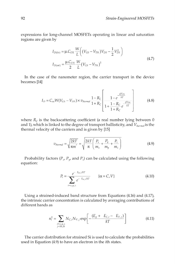
expressions for long-channel MOSFETs operating in linear and saturation
regions are given by
.
1
2
.
2
( )
2
( )
2
I
C
W
L
V
V V
V
I
C W
L
V
V
D lin
OX
GS
TH
DS
DS
D sat
OX
GS
TH
(
)
(
)
= µ
−
−
=
µ
−
(4.7)
In the case of the nanometer region, the carrier transport in the device
becomes [14]
(
)
1
1
1
1
1
1
I
C W V
V
v
R
R
e
R
R
e
D
o x
G S
T H
t hermal
C
C
qV
kT
C
C
qV
kT
DS
DS
=
−
×
−
+
−
+
−
+
−
−
(4.8)
where R C is the backscattering coefficient (a real number lying between 0
and 1), which is linked to the degree of transport ballisticity, and V thermal is the
thermal velocity of the carriers and is given by [15]
2
2
*
v
kT
m
kT P
m
P
m
P
m
thermal
x
x
y
y
z
z
= π
=
π
+
+
(4.9)
Probability factors (P x , P y , and P z ) can be calculated using the following
equation:
{
, }
/
/
, ,
,
,
P
e
e
C V
i
E
kT
E
kT
i x y z
i
i
∑
=
α =
−
−
=
α
α
(4.10)
Using a strained-induced band structure from Equations (4.16) and (4.17),
the intrinsic carrier concentration is calculated by averaging contributions of
different bands as
exp
(
)
2
,
,
,
,
, ,
,
n
N N
E
E
E
kT
i
C i V j
g
Ci
Vj
i x y z
j hh lh
∑
=
−
+
−
=
=
(4.11)
The carrier distribution for strained Si is used to calculate the probabilities
used in Equation (4.9) to have an electron in the ith states.
Strain-Engineered MOSFETs
expressions for long-channel MOSFETs operating in linear and saturation
regions are given by
.
1
2
.
2
( )
2
( )
2
I
C
W
L
V
V V
V
I
C W
L
V
V
D lin
OX
GS
TH
DS
DS
D sat
OX
GS
TH
(
)
(
)
= µ
−
−
=
µ
−
(4.7)
In the case of the nanometer region, the carrier transport in the device
becomes [14]
(
)
1
1
1
1
1
1
I
C W V
V
v
R
R
e
R
R
e
D
o x
G S
T H
t hermal
C
C
qV
kT
C
C
qV
kT
DS
DS
=
−
×
−
+
−
+
−
+
−
−
(4.8)
where R C is the backscattering coefficient (a real number lying between 0
and 1), which is linked to the degree of transport ballisticity, and V thermal is the
thermal velocity of the carriers and is given by [15]
2
2
*
v
kT
m
kT P
m
P
m
P
m
thermal
x
x
y
y
z
z
= π
=
π
+
+
(4.9)
Probability factors (P x , P y , and P z ) can be calculated using the following
equation:
{
, }
/
/
, ,
,
,
P
e
e
C V
i
E
kT
E
kT
i x y z
i
i
∑
=
α =
−
−
=
α
α
(4.10)
Using a strained-induced band structure from Equations (4.16) and (4.17),
the intrinsic carrier concentration is calculated by averaging contributions of
different bands as
exp
(
)
2
,
,
,
,
, ,
,
n
N N
E
E
E
kT
i
C i V j
g
Ci
Vj
i x y z
j hh lh
∑
=
−
+
−
=
=
(4.11)
The carrier distribution for strained Si is used to calculate the probabilities
used in Equation (4.9) to have an electron in the ith states.