

89
Electronic Properties of Strain-Engineered Semiconductors
4.1 Basics of Stress Engineering
Since the primary focus is on strain-engineered MOSFETs, it is essential
to understand the basics of engineering mechanics like stress, strain, and
mechanical properties of the semiconductor involved. Within the elastic
limit, the property of solid materials to deform under the application of an
external force and to regain their original shape after the force is removed
is referred to as elasticity. It is Hooke’s law, which describes the elastic
relationship between the mechanical constraint and deformation that the
material will undergo. The external force applied on a specified area is
known as stress, while the amount of deformation is called the strain. In
the following, the theory of stress, strain, and their interdependence is
briefly discussed.
4.1.1 Stress
The stress (σ) at a point may be determined by considering a small element
of the body enclosed by area (ΔA) on which forces act (ΔP), and its unit is
Pascal (Pa). By making the element infinitesimally small, the stress (σ) vector
is defined as the limit
lim
0
F
A
dF
dA
A
σ =
=
→
(4.1)
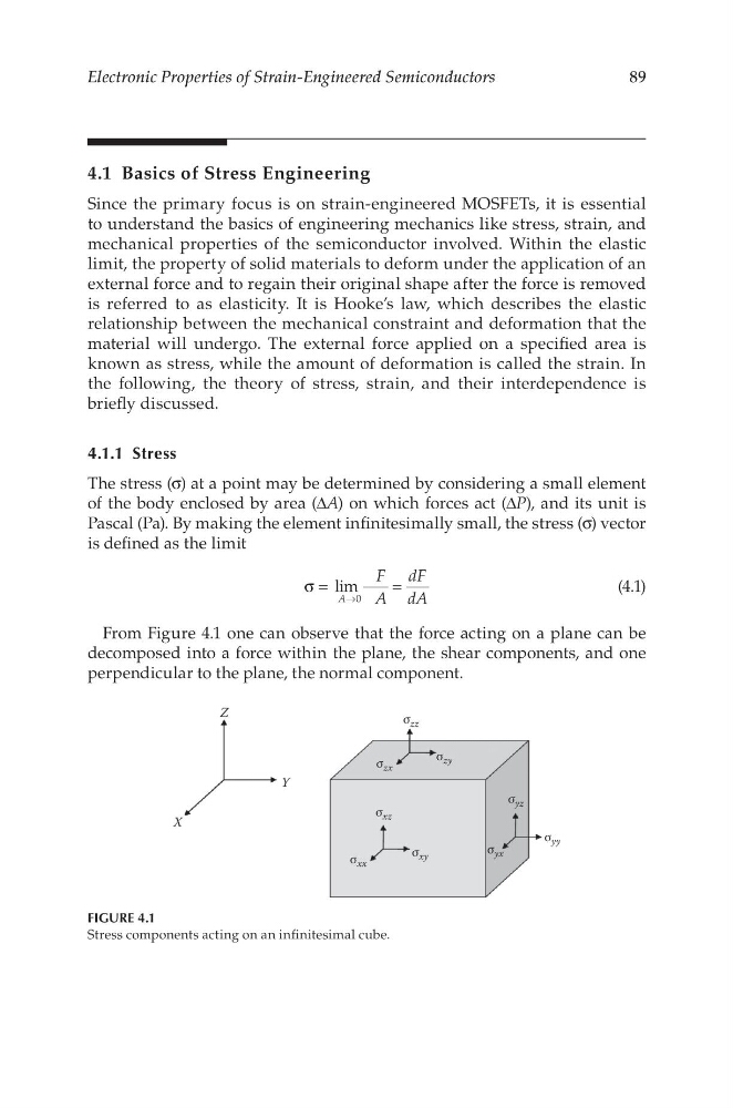
From Figure 4.1 one can observe that the force acting on a plane can be
decomposed into a force within the plane, the shear components, and one
perpendicular to the plane, the normal component.
Z
X
Y
σ zz
σ zx
σ zy
σ xz
σ xx
σ xy
σ yz
σ yx
σ yy
FIGURE 4.1
Stress components acting on an infinitesimal cube.
Electronic Properties of Strain-Engineered Semiconductors
4.1 Basics of Stress Engineering
Since the primary focus is on strain-engineered MOSFETs, it is essential
to understand the basics of engineering mechanics like stress, strain, and
mechanical properties of the semiconductor involved. Within the elastic
limit, the property of solid materials to deform under the application of an
external force and to regain their original shape after the force is removed
is referred to as elasticity. It is Hooke’s law, which describes the elastic
relationship between the mechanical constraint and deformation that the
material will undergo. The external force applied on a specified area is
known as stress, while the amount of deformation is called the strain. In
the following, the theory of stress, strain, and their interdependence is
briefly discussed.
4.1.1 Stress
The stress (σ) at a point may be determined by considering a small element
of the body enclosed by area (ΔA) on which forces act (ΔP), and its unit is
Pascal (Pa). By making the element infinitesimally small, the stress (σ) vector
is defined as the limit
lim
0
F
A
dF
dA
A
σ =
=
→
(4.1)
From Figure 4.1 one can observe that the force acting on a plane can be
decomposed into a force within the plane, the shear components, and one
perpendicular to the plane, the normal component.
Z
X
Y
σ zz
σ zx
σ zy
σ xz
σ xx
σ xy
σ yz
σ yx
σ yy
FIGURE 4.1
Stress components acting on an infinitesimal cube.