

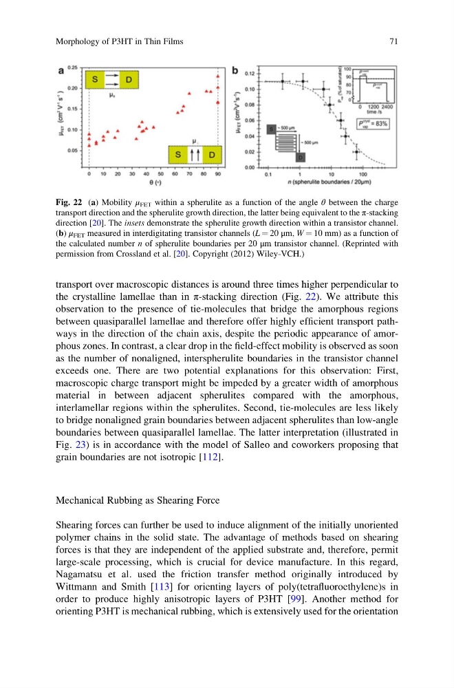
transport over macroscopic distances is around three times higher perpendicular to
the crystalline lamellae than in π-stacking direction (Fig. 22). We attribute this
observation to the presence of tie-molecules that bridge the amorphous regions
between quasiparallel lamellae and therefore offer highly efficient transport pathways in the direction of the chain axis, despite the periodic appearance of amorphous zones. In contrast, a clear drop in the field-effect mobility is observed as soon
as the number of nonaligned, interspherulite boundaries in the transistor channel
exceeds one. There are two potential explanations for this observation: First,
macroscopic charge transport might be impeded by a greater width of amorphous
material in between adjacent spherulites compared with the amorphous,
interlamellar regions within the spherulites. Second, tie-molecules are less likely
to bridge nonaligned grain boundaries between adjacent spherulites than low-angle
boundaries between quasiparallel lamellae. The latter interpretation (illustrated in
Fig. 23) is in accordance with the model of Salleo and coworkers proposing that
grain boundaries are not isotropic [112].
Mechanical Rubbing as Shearing Force
Shearing forces can further be used to induce alignment of the initially unoriented
polymer chains in the solid state. The advantage of methods based on shearing
forces is that they are independent of the applied substrate and, therefore, permit
large-scale processing, which is crucial for device manufacture. In this regard,
Nagamatsu et al. used the friction transfer method originally introduced by
Wittmann and Smith [113] for orienting layers of poly(tetrafluoroethylene)s in
order to produce highly anisotropic layers of P3HT [99]. Another method for
orienting P3HT is mechanical rubbing, which is extensively used for the orientation
Fig. 22 (a) Mobility μ FET within a spherulite as a function of the angle θ between the charge
transport direction and the spherulite growth direction, the latter being equivalent to the π-stacking
direction [20]. The insets demonstrate the spherulite growth direction within a transistor channel.
(b) μ FET measured in interdigitating transistor channels (L ¼ 20 μm, W ¼ 10 mm) as a function of
the calculated number n of spherulite boundaries per 20 μm transistor channel. (Reprinted with
permission from Crossland et al. [20]. Copyright (2012) Wiley-VCH.)
Morphology of P3HT in Thin Films
71
the crystalline lamellae than in π-stacking direction (Fig. 22). We attribute this
observation to the presence of tie-molecules that bridge the amorphous regions
between quasiparallel lamellae and therefore offer highly efficient transport pathways in the direction of the chain axis, despite the periodic appearance of amorphous zones. In contrast, a clear drop in the field-effect mobility is observed as soon
as the number of nonaligned, interspherulite boundaries in the transistor channel
exceeds one. There are two potential explanations for this observation: First,
macroscopic charge transport might be impeded by a greater width of amorphous
material in between adjacent spherulites compared with the amorphous,
interlamellar regions within the spherulites. Second, tie-molecules are less likely
to bridge nonaligned grain boundaries between adjacent spherulites than low-angle
boundaries between quasiparallel lamellae. The latter interpretation (illustrated in
Fig. 23) is in accordance with the model of Salleo and coworkers proposing that
grain boundaries are not isotropic [112].
Mechanical Rubbing as Shearing Force
Shearing forces can further be used to induce alignment of the initially unoriented
polymer chains in the solid state. The advantage of methods based on shearing
forces is that they are independent of the applied substrate and, therefore, permit
large-scale processing, which is crucial for device manufacture. In this regard,
Nagamatsu et al. used the friction transfer method originally introduced by
Wittmann and Smith [113] for orienting layers of poly(tetrafluoroethylene)s in
order to produce highly anisotropic layers of P3HT [99]. Another method for
orienting P3HT is mechanical rubbing, which is extensively used for the orientation
Fig. 22 (a) Mobility μ FET within a spherulite as a function of the angle θ between the charge
transport direction and the spherulite growth direction, the latter being equivalent to the π-stacking
direction [20]. The insets demonstrate the spherulite growth direction within a transistor channel.
(b) μ FET measured in interdigitating transistor channels (L ¼ 20 μm, W ¼ 10 mm) as a function of
the calculated number n of spherulite boundaries per 20 μm transistor channel. (Reprinted with
permission from Crossland et al. [20]. Copyright (2012) Wiley-VCH.)
Morphology of P3HT in Thin Films
71