

which the current flowing through the channel is directly proportional to V DS and
the charge carrier mobility μ lin and can be described by:
I DS lin
ð Þ ¼
W
L
Á C i Á μ lin Á V G À V Th
ð
ÞÁV DS
ð1Þ
If the source-drain voltage is further increased, a point will be reached where
V DS ¼ V G À V Th . At this point the channel is ‘pinched off.’ That is, the local
potential at the drain electrode is lower than the threshold voltage and a depletion
region forms next to the drain. A space charge limited current can flow across this
narrow depletion zone. Charge carriers are swept from the pinch-off point to the
drain by the comparatively high electric field across the depletion region. Any
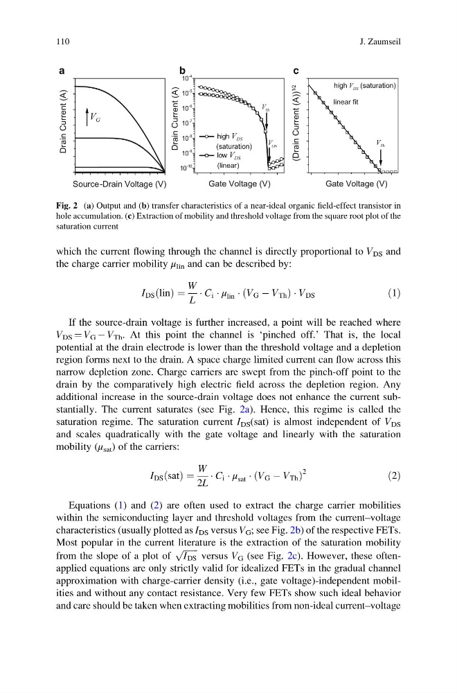
additional increase in the source-drain voltage does not enhance the current substantially. The current saturates (see Fig. 2a). Hence, this regime is called the
saturation regime. The saturation current I DS (sat) is almost independent of V DS
and scales quadratically with the gate voltage and linearly with the saturation
mobility (μ sat ) of the carriers:
I DS sat
ð Þ ¼
W
2L
Á C i Á μ sat Á V G À V Th
ð
Þ
2
ð2Þ
Equations (1) and (2) are often used to extract the charge carrier mobilities
within the semiconducting layer and threshold voltages from the current–voltage
characteristics (usually plotted as I DS versus V G ; see Fig. 2b) of the respective FETs.
Most popular in the current literature is the extraction of the saturation mobility
from the slope of a plot of
ffiffiffiffiffiffi ffi
I DS
p
versus V G (see Fig. 2c). However, these oftenapplied equations are only strictly valid for idealized FETs in the gradual channel
approximation with charge-carrier density (i.e., gate voltage)-independent mobilities and without any contact resistance. Very few FETs show such ideal behavior
and care should be taken when extracting mobilities from non-ideal current–voltage
Drain Current (A)
Source-Drain Voltage (V)
V G
a
10
-10
10
-9
10
-8
10
-7
10
-6
10
-5
10
-4
V ON
high V DS
(saturation)
low V DS
(linear)
Drain Current (A)
Gate Voltage (V)
V Th
b
linear fit
high V DS (saturation)
(Drain Current (A))
1/2
Gate Voltage (V)
V Th
c
Fig. 2 (a) Output and (b) transfer characteristics of a near-ideal organic field-effect transistor in
hole accumulation. (c) Extraction of mobility and threshold voltage from the square root plot of the
saturation current
110
J. Zaumseil
the charge carrier mobility μ lin and can be described by:
I DS lin
ð Þ ¼
W
L
Á C i Á μ lin Á V G À V Th
ð
ÞÁV DS
ð1Þ
If the source-drain voltage is further increased, a point will be reached where
V DS ¼ V G À V Th . At this point the channel is ‘pinched off.’ That is, the local
potential at the drain electrode is lower than the threshold voltage and a depletion
region forms next to the drain. A space charge limited current can flow across this
narrow depletion zone. Charge carriers are swept from the pinch-off point to the
drain by the comparatively high electric field across the depletion region. Any
additional increase in the source-drain voltage does not enhance the current substantially. The current saturates (see Fig. 2a). Hence, this regime is called the
saturation regime. The saturation current I DS (sat) is almost independent of V DS
and scales quadratically with the gate voltage and linearly with the saturation
mobility (μ sat ) of the carriers:
I DS sat
ð Þ ¼
W
2L
Á C i Á μ sat Á V G À V Th
ð
Þ
2
ð2Þ
Equations (1) and (2) are often used to extract the charge carrier mobilities
within the semiconducting layer and threshold voltages from the current–voltage
characteristics (usually plotted as I DS versus V G ; see Fig. 2b) of the respective FETs.
Most popular in the current literature is the extraction of the saturation mobility
from the slope of a plot of
ffiffiffiffiffiffi ffi
I DS
p
versus V G (see Fig. 2c). However, these oftenapplied equations are only strictly valid for idealized FETs in the gradual channel
approximation with charge-carrier density (i.e., gate voltage)-independent mobilities and without any contact resistance. Very few FETs show such ideal behavior
and care should be taken when extracting mobilities from non-ideal current–voltage
Drain Current (A)
Source-Drain Voltage (V)
V G
a
10
-10
10
-9
10
-8
10
-7
10
-6
10
-5
10
-4
V ON
high V DS
(saturation)
low V DS
(linear)
Drain Current (A)
Gate Voltage (V)
V Th
b
linear fit
high V DS (saturation)
(Drain Current (A))
1/2
Gate Voltage (V)
V Th
c
Fig. 2 (a) Output and (b) transfer characteristics of a near-ideal organic field-effect transistor in
hole accumulation. (c) Extraction of mobility and threshold voltage from the square root plot of the
saturation current
110
J. Zaumseil