

Voltage is applied to the gate electrode (gate voltage, V G ) and the drain electrode
(V D ). The source electrode is usually grounded (V S ¼ 0). The potential difference
between source and drain is referred to as the source-drain voltage (V DS ). The
source is the charge injecting electrode. When a positive gate voltage is applied
with respect to the source, electrons are injected. When a negative gate voltage is
applied, holes are injected. The applied gate voltage determines the amount of
accumulated charges in the channel and thus the current flow between the source
and the drain electrode (source-drain current, I DS ), which is the product of charge
carrier density, mobility, and the lateral electric field. The number of accumulated
charges in the channel is proportional to V G and the areal capacitance C i of the
insulator. Note that charges only accumulate within a very short distance from the
semiconductor–dielectric interface, usually within the first molecular layer. Not all
induced charges are mobile and contribute to the current in an FET. Any existing
deep trap states first have to be filled before the induced charges can become
mobile. That is, a gate voltage higher than a so-called threshold voltage V Th must
be applied and thus the effective voltage for calculating the amount of mobile
charges is V G À V Th . On the other hand, unintentional doping (e.g, by impurities)
can cause charges to already be present in the channel when V G ¼ 0 and an opposite
voltage has to be applied to turn the channel off. We will see that this is often the
case for P3HT-FETs.
When a small source-drain voltage (i.e., a lateral electric field) is applied
(V DS ( V G ), charges move from the injecting source to the drain electrode. A linear
gradient of charge density forms and current flows. This is the linear regime, in
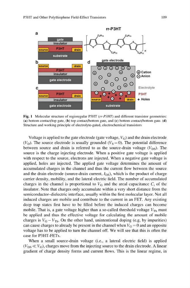
Fig. 1 Molecular structure of regioregular P3HT (rr-P3HT) and different transistor geometries:
(a) bottom contact/top gate, (b) top contact/bottom gate, and (c) bottom contact/bottom gate. (d)
Structure and working principle of electrolyte-gated, electrochemical transistors
P3HT and Other Polythiophene Field-Effect Transistors
109
(V D ). The source electrode is usually grounded (V S ¼ 0). The potential difference
between source and drain is referred to as the source-drain voltage (V DS ). The
source is the charge injecting electrode. When a positive gate voltage is applied
with respect to the source, electrons are injected. When a negative gate voltage is
applied, holes are injected. The applied gate voltage determines the amount of
accumulated charges in the channel and thus the current flow between the source
and the drain electrode (source-drain current, I DS ), which is the product of charge
carrier density, mobility, and the lateral electric field. The number of accumulated
charges in the channel is proportional to V G and the areal capacitance C i of the
insulator. Note that charges only accumulate within a very short distance from the
semiconductor–dielectric interface, usually within the first molecular layer. Not all
induced charges are mobile and contribute to the current in an FET. Any existing
deep trap states first have to be filled before the induced charges can become
mobile. That is, a gate voltage higher than a so-called threshold voltage V Th must
be applied and thus the effective voltage for calculating the amount of mobile
charges is V G À V Th . On the other hand, unintentional doping (e.g, by impurities)
can cause charges to already be present in the channel when V G ¼ 0 and an opposite
voltage has to be applied to turn the channel off. We will see that this is often the
case for P3HT-FETs.
When a small source-drain voltage (i.e., a lateral electric field) is applied
(V DS ( V G ), charges move from the injecting source to the drain electrode. A linear
gradient of charge density forms and current flows. This is the linear regime, in
Fig. 1 Molecular structure of regioregular P3HT (rr-P3HT) and different transistor geometries:
(a) bottom contact/top gate, (b) top contact/bottom gate, and (c) bottom contact/bottom gate. (d)
Structure and working principle of electrolyte-gated, electrochemical transistors
P3HT and Other Polythiophene Field-Effect Transistors
109