

5.4 Nano-optoelectronics
Organic photodiodes and phototransistors are fabricated by using photosensitive
π-conjugated organic materials, and the photovoltaic properties of these materials
have been intensively studied for application to inexpensive and renewable energy
sources [140]. The mechanism of charge recombination and dissociation in the p–n
junctions of semiconductors is used in various applications such as diode lasers,
LEDs, photodetectors, and photovoltaic cells. With the rapid development of
nanotechnology, nanoscale p–n junctions have been investigated by using lowdimensional nanostructures such as carbon nanotubes (CNTs) and inorganic or
organic semiconducting NWs.
A doped Si substrate with as-grown multiwalled (MW) CNTs synthesized through
a thermal chemical vapor deposition (CVD) method was attached to a stainless steel
working electrode, as shown in Fig. 27a [141]. A P3HT layer with a thickness of
~20 nm was directly deposited on the surface of the MWCNTs using an electrochemical polymerization method. The electrolyte for the electrochemical polymerization
consisted of 3-HT monomers, BMIMPF 6 as the ionic liquid, and anhydrous acetonitrile as the solvent.
The formation and surface morphology of the coaxial P3HT/MWCNT hybrid
NTs were investigated using HR-TEM, as shown in Fig. 27b [141]. The MWCNTs
had an outer diameter of 10À30 nm and a wall thickness of 2À8 nm. The total
diameter of the hybrid NTs was ~60 nm. The thickness of the P3HT layer deposited
on the MWCNTs was ~20 (Æ10) nm, and the formation of the coaxial-type
MWCNTs coated with P3HT was clearly observed.
Figure 27c shows a schematic illustration of the four-probe electrodes on a
P3HT/MWCNT hybrid single NT. Two Au/Ti electrodes make contact with the
outer P3HT single NT, while the other two make contact with the inner single
a
b
PL Intensity (arb. unit)
0
100 aM
P3MT/
p-DNA NW
P3MT NW
800
Wavelength (nm)
900
700
600
500
100 nM
1 nM
1 pM
1 fM
Wavelength (nm)
900
800
700
600
500
5
10
15
20
25
30
35
0.0
0.5
1.0
1.5
2.0
2.5
PL Intensity (arb. unit)
a
P3MT (TBACF 3 SO 3 ) /
p-DNA + t-DNA NW
P3MT (TBACF 3 SO 3 ) NW
P3MT
(TBACF3SO3) /
p-DNA NW
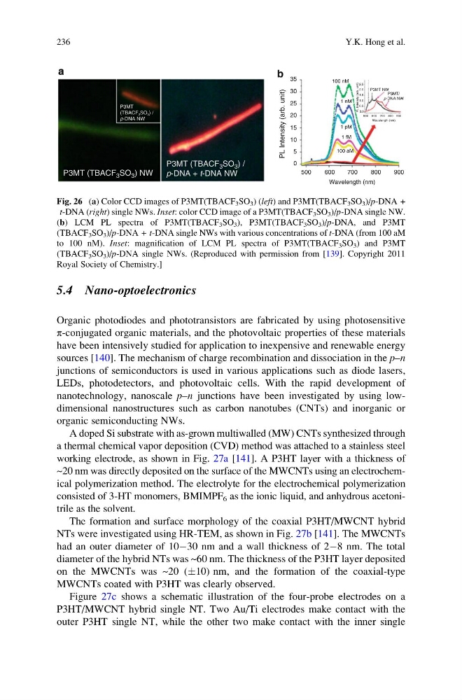
Fig. 26 (a) Color CCD images of P3MT(TBACF 3 SO 3 ) (left) and P3MT(TBACF 3 SO 3 )/p-DNA +
t-DNA (right) single NWs. Inset: color CCD image of a P3MT(TBACF 3 SO 3 )/p-DNA single NW.
(b) LCM PL spectra of P3MT(TBACF 3 SO 3 ), P3MT(TBACF 3 SO 3 )/p-DNA, and P3MT
(TBACF 3 SO 3 )/p-DNA + t-DNA single NWs with various concentrations of t-DNA (from 100 aM
to 100 nM). Inset: magnification of LCM PL spectra of P3MT(TBACF 3 SO 3 ) and P3MT
(TBACF 3 SO 3 )/p-DNA single NWs. (Reproduced with permission from [139]. Copyright 2011
Royal Society of Chemistry.]
236
Y.K. Hong et al.
Organic photodiodes and phototransistors are fabricated by using photosensitive
π-conjugated organic materials, and the photovoltaic properties of these materials
have been intensively studied for application to inexpensive and renewable energy
sources [140]. The mechanism of charge recombination and dissociation in the p–n
junctions of semiconductors is used in various applications such as diode lasers,
LEDs, photodetectors, and photovoltaic cells. With the rapid development of
nanotechnology, nanoscale p–n junctions have been investigated by using lowdimensional nanostructures such as carbon nanotubes (CNTs) and inorganic or
organic semiconducting NWs.
A doped Si substrate with as-grown multiwalled (MW) CNTs synthesized through
a thermal chemical vapor deposition (CVD) method was attached to a stainless steel
working electrode, as shown in Fig. 27a [141]. A P3HT layer with a thickness of
~20 nm was directly deposited on the surface of the MWCNTs using an electrochemical polymerization method. The electrolyte for the electrochemical polymerization
consisted of 3-HT monomers, BMIMPF 6 as the ionic liquid, and anhydrous acetonitrile as the solvent.
The formation and surface morphology of the coaxial P3HT/MWCNT hybrid
NTs were investigated using HR-TEM, as shown in Fig. 27b [141]. The MWCNTs
had an outer diameter of 10À30 nm and a wall thickness of 2À8 nm. The total
diameter of the hybrid NTs was ~60 nm. The thickness of the P3HT layer deposited
on the MWCNTs was ~20 (Æ10) nm, and the formation of the coaxial-type
MWCNTs coated with P3HT was clearly observed.
Figure 27c shows a schematic illustration of the four-probe electrodes on a
P3HT/MWCNT hybrid single NT. Two Au/Ti electrodes make contact with the
outer P3HT single NT, while the other two make contact with the inner single
a
b
PL Intensity (arb. unit)
0
100 aM
P3MT/
p-DNA NW
P3MT NW
800
Wavelength (nm)
900
700
600
500
100 nM
1 nM
1 pM
1 fM
Wavelength (nm)
900
800
700
600
500
5
10
15
20
25
30
35
0.0
0.5
1.0
1.5
2.0
2.5
PL Intensity (arb. unit)
a
P3MT (TBACF 3 SO 3 ) /
p-DNA + t-DNA NW
P3MT (TBACF 3 SO 3 ) NW
P3MT
(TBACF3SO3) /
p-DNA NW
Fig. 26 (a) Color CCD images of P3MT(TBACF 3 SO 3 ) (left) and P3MT(TBACF 3 SO 3 )/p-DNA +
t-DNA (right) single NWs. Inset: color CCD image of a P3MT(TBACF 3 SO 3 )/p-DNA single NW.
(b) LCM PL spectra of P3MT(TBACF 3 SO 3 ), P3MT(TBACF 3 SO 3 )/p-DNA, and P3MT
(TBACF 3 SO 3 )/p-DNA + t-DNA single NWs with various concentrations of t-DNA (from 100 aM
to 100 nM). Inset: magnification of LCM PL spectra of P3MT(TBACF 3 SO 3 ) and P3MT
(TBACF 3 SO 3 )/p-DNA single NWs. (Reproduced with permission from [139]. Copyright 2011
Royal Society of Chemistry.]
236
Y.K. Hong et al.