

378
11 Templated Systems
the transport properties of nanowire arrays, the back side electrical contact used as
working electrode connection during the nanowire deposition can serve as one of the
electrical contacts, while the solution side of the nanowires can be contacted either
through the percolating overgrown deposit or with electrically conducting glue. This
method makes it possible to measure the average of the transport properties of a
large number of nanowires. If the template is removed, single nanowires can be
contacted with a micromanipulating system in a SEM device, mostly on lithographically patterned electrical contact pads. Below, we will pay attention to methods
dealing with single nanowire still within the template because the preparation of the
systems to be measured involves an electrochemical step in excess to the nanowire
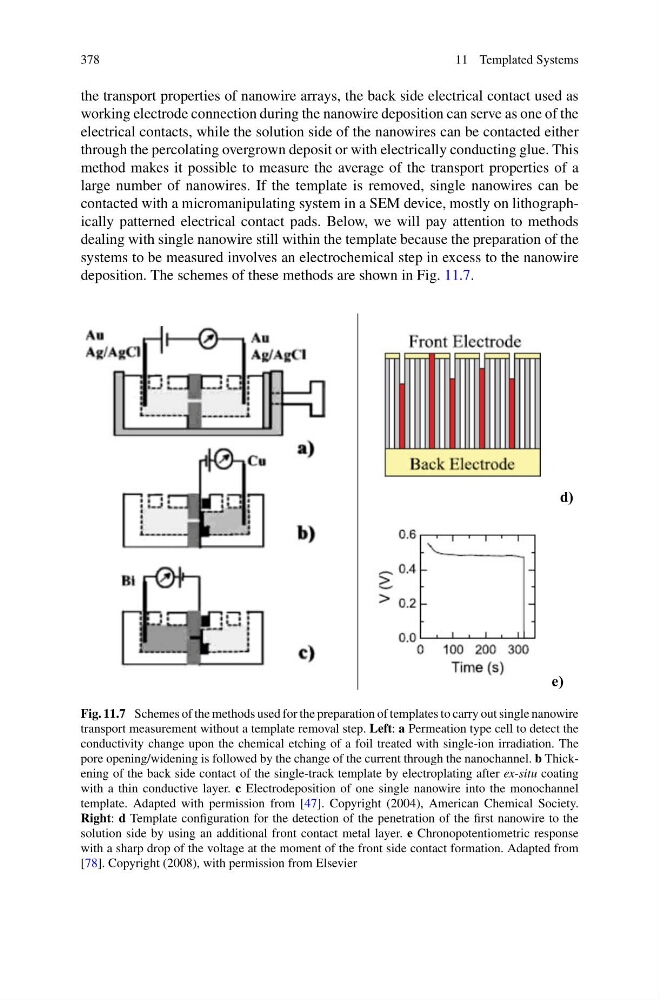
deposition. The schemes of these methods are shown in Fig. 11.7.
d)
e)
Fig. 11.7 Schemes of the methods used for the preparation of templates to carry out single nanowire
transport measurement without a template removal step. Left: a Permeation type cell to detect the
conductivity change upon the chemical etching of a foil treated with single-ion irradiation. The
pore opening/widening is followed by the change of the current through the nanochannel. b Thickening of the back side contact of the single-track template by electroplating after ex-situ coating
with a thin conductive layer. c Electrodeposition of one single nanowire into the monochannel
template. Adapted with permission from [47]. Copyright (2004), American Chemical Society.
Right: d Template configuration for the detection of the penetration of the first nanowire to the
solution side by using an additional front contact metal layer. e Chronopotentiometric response
with a sharp drop of the voltage at the moment of the front side contact formation. Adapted from
[78]. Copyright (2008), with permission from Elsevier
11 Templated Systems
the transport properties of nanowire arrays, the back side electrical contact used as
working electrode connection during the nanowire deposition can serve as one of the
electrical contacts, while the solution side of the nanowires can be contacted either
through the percolating overgrown deposit or with electrically conducting glue. This
method makes it possible to measure the average of the transport properties of a
large number of nanowires. If the template is removed, single nanowires can be
contacted with a micromanipulating system in a SEM device, mostly on lithographically patterned electrical contact pads. Below, we will pay attention to methods
dealing with single nanowire still within the template because the preparation of the
systems to be measured involves an electrochemical step in excess to the nanowire
deposition. The schemes of these methods are shown in Fig. 11.7.
d)
e)
Fig. 11.7 Schemes of the methods used for the preparation of templates to carry out single nanowire
transport measurement without a template removal step. Left: a Permeation type cell to detect the
conductivity change upon the chemical etching of a foil treated with single-ion irradiation. The
pore opening/widening is followed by the change of the current through the nanochannel. b Thickening of the back side contact of the single-track template by electroplating after ex-situ coating
with a thin conductive layer. c Electrodeposition of one single nanowire into the monochannel
template. Adapted with permission from [47]. Copyright (2004), American Chemical Society.
Right: d Template configuration for the detection of the penetration of the first nanowire to the
solution side by using an additional front contact metal layer. e Chronopotentiometric response
with a sharp drop of the voltage at the moment of the front side contact formation. Adapted from
[78]. Copyright (2008), with permission from Elsevier