

118
4 Ultrathin Layers
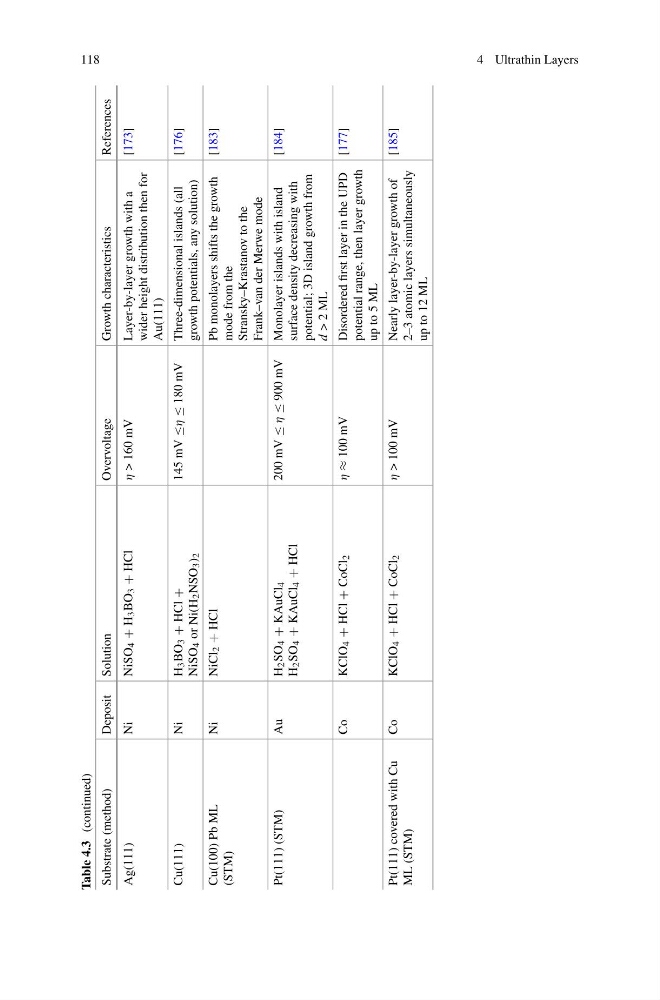
Table 4.3
(continued)
Substrate (method)
Deposit Solution
Overvoltage
Growth characteristics
References
Ag(111)
Ni
NiSO
4
+ H
3 BO
3
+ HCl
η > 160 mV
Layer-by-layer growth with a
wider height distribution then for
Au(111)
[173]
Cu(111)
Ni
H
3 BO
3
+ HCl
+
NiSO
4 or Ni(H
2 NSO
3 )
2
145 mV
≤η ≤ 180 mV
Three-dimensional islands (all
growth potentials, any solution)
[176]
Cu(100) Pb ML
(STM)
Ni
NiCl
2
+ HCl
Pb monolayers shifts the growth
mode from the
Stransky–Krastanov to the
Frank–van der Merwe mode
[183]
Pt(111) (STM)
Au
H
2 SO
4
+ KAuCl
4
H
2 SO
4
+ KAuCl
4
+ HCl
200 mV
≤ η ≤ 900 mV Monolayer islands with island
surface density decreasing with
potential; 3D island growth from
d
> 2 ML
[184]
Co
KClO
4
+ HCl
+ CoCl
2
η ≈ 100 mV
Disordered first layer in the UPD
potential range, then layer growth
up to 5 ML
[177]
Pt(111) covered with Cu
ML (STM)
Co
KClO
4
+ HCl
+ CoCl
2
η > 100 mV
Nearly layer-by-layer growth of
2–3 atomic layers simultaneously
up to 12 ML
[185]
4 Ultrathin Layers
Table 4.3
(continued)
Substrate (method)
Deposit Solution
Overvoltage
Growth characteristics
References
Ag(111)
Ni
NiSO
4
+ H
3 BO
3
+ HCl
η > 160 mV
Layer-by-layer growth with a
wider height distribution then for
Au(111)
[173]
Cu(111)
Ni
H
3 BO
3
+ HCl
+
NiSO
4 or Ni(H
2 NSO
3 )
2
145 mV
≤η ≤ 180 mV
Three-dimensional islands (all
growth potentials, any solution)
[176]
Cu(100) Pb ML
(STM)
Ni
NiCl
2
+ HCl
Pb monolayers shifts the growth
mode from the
Stransky–Krastanov to the
Frank–van der Merwe mode
[183]
Pt(111) (STM)
Au
H
2 SO
4
+ KAuCl
4
H
2 SO
4
+ KAuCl
4
+ HCl
200 mV
≤ η ≤ 900 mV Monolayer islands with island
surface density decreasing with
potential; 3D island growth from
d
> 2 ML
[184]
Co
KClO
4
+ HCl
+ CoCl
2
η ≈ 100 mV
Disordered first layer in the UPD
potential range, then layer growth
up to 5 ML
[177]
Pt(111) covered with Cu
ML (STM)
Co
KClO
4
+ HCl
+ CoCl
2
η > 100 mV
Nearly layer-by-layer growth of
2–3 atomic layers simultaneously
up to 12 ML
[185]