

4.2 Combination of UPD with Other Surface-Area-Limited Processes
101
a
b
d
c
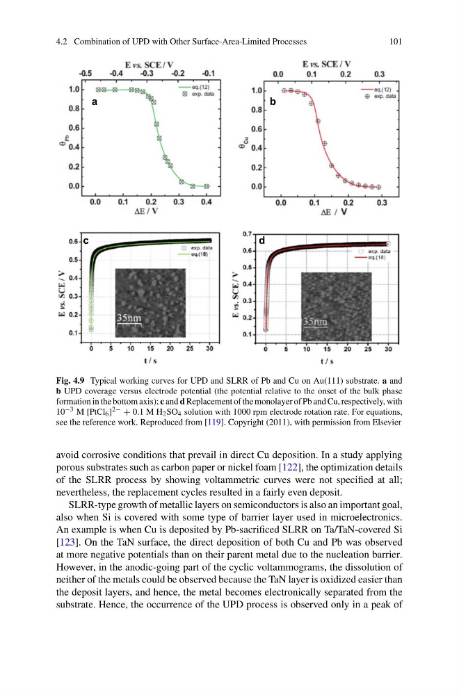
Fig. 4.9 Typical working curves for UPD and SLRR of Pb and Cu on Au(111) substrate. a and
b UPD coverage versus electrode potential (the potential relative to the onset of the bulk phase
formation in the bottom axis); c and d Replacement of the monolayer of Pb and Cu, respectively, with
10 −3 M [PtCl 6 ] 2− + 0.1 M H 2 SO 4 solution with 1000 rpm electrode rotation rate. For equations,
see the reference work. Reproduced from [119]. Copyright (2011), with permission from Elsevier
avoid corrosive conditions that prevail in direct Cu deposition. In a study applying
porous substrates such as carbon paper or nickel foam [122], the optimization details
of the SLRR process by showing voltammetric curves were not specified at all;
nevertheless, the replacement cycles resulted in a fairly even deposit.
SLRR-type growth of metallic layers on semiconductors is also an important goal,
also when Si is covered with some type of barrier layer used in microelectronics.
An example is when Cu is deposited by Pb-sacrificed SLRR on Ta/TaN-covered Si
[123]. On the TaN surface, the direct deposition of both Cu and Pb was observed
at more negative potentials than on their parent metal due to the nucleation barrier.
However, in the anodic-going part of the cyclic voltammograms, the dissolution of
neither of the metals could be observed because the TaN layer is oxidized easier than
the deposit layers, and hence, the metal becomes electronically separated from the
substrate. Hence, the occurrence of the UPD process is observed only in a peak of
101
a
b
d
c
Fig. 4.9 Typical working curves for UPD and SLRR of Pb and Cu on Au(111) substrate. a and
b UPD coverage versus electrode potential (the potential relative to the onset of the bulk phase
formation in the bottom axis); c and d Replacement of the monolayer of Pb and Cu, respectively, with
10 −3 M [PtCl 6 ] 2− + 0.1 M H 2 SO 4 solution with 1000 rpm electrode rotation rate. For equations,
see the reference work. Reproduced from [119]. Copyright (2011), with permission from Elsevier
avoid corrosive conditions that prevail in direct Cu deposition. In a study applying
porous substrates such as carbon paper or nickel foam [122], the optimization details
of the SLRR process by showing voltammetric curves were not specified at all;
nevertheless, the replacement cycles resulted in a fairly even deposit.
SLRR-type growth of metallic layers on semiconductors is also an important goal,
also when Si is covered with some type of barrier layer used in microelectronics.
An example is when Cu is deposited by Pb-sacrificed SLRR on Ta/TaN-covered Si
[123]. On the TaN surface, the direct deposition of both Cu and Pb was observed
at more negative potentials than on their parent metal due to the nucleation barrier.
However, in the anodic-going part of the cyclic voltammograms, the dissolution of
neither of the metals could be observed because the TaN layer is oxidized easier than
the deposit layers, and hence, the metal becomes electronically separated from the
substrate. Hence, the occurrence of the UPD process is observed only in a peak of