

94
4 Ultrathin Layers
a
b
c
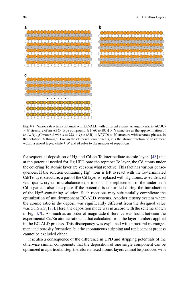
Fig. 4.7 Various structures obtained with EC-ALD with different atomic arrangements. a (ACBC)
× N structure of an ABC 2 type compound, b [(AC) k (BC)] × N structure as the approximation of
an A x B 1−x C material with x = k/(k + 1); c (AB) × N/(CD) × M structure with separate phases. In
the notation, A through D mean the elemental components, x is the atomic fraction of an element
within a mixed layer, while k, N and M refer to the number of repetitions
for sequential deposition of Hg and Cd on Te intermediate atomic layers [48] that
at the potential needed for Hg UPD onto the topmost Te layer, the Cd atoms under
the covering Te atomic layer are yet somewhat reactive. This fact has various consequences. If the solution containing Hg
2+ ions is left to react with the Te-terminated
Cd/Te layer structure, a part of the Cd layer is replaced with Hg atoms, as evidenced
with quartz crystal microbalance experiments. The replacement of the underneath
Cd layer can also take place if the potential is controlled during the introduction
of the Hg
2+ -containing solution. Such reactions may substantially complicate the
optimization of multicomponent EC-ALD systems. Another ternary system where
the atomic ratio in the deposit was significantly different from the designed value
was Cu x Sn y S z [83]. Here, the deposition mode was in accord with the scheme shown
in Fig. 4.7b. As much as an order of magnitude difference was found between the
experimental Cu/Sn atomic ratio and that calculated from the layer numbers applied
in the EC-ALD process. This discrepancy was explained with structural rearrangement and porosity formation, but the spontaneous stripping and replacement process
cannot be excluded either.
It is also a consequence of the difference in UPD and stripping potentials of the
otherwise similar components that the deposition of one single component can be
optimized in a particular step; therefore, mixed atomic layers cannot be produced with
4 Ultrathin Layers
a
b
c
Fig. 4.7 Various structures obtained with EC-ALD with different atomic arrangements. a (ACBC)
× N structure of an ABC 2 type compound, b [(AC) k (BC)] × N structure as the approximation of
an A x B 1−x C material with x = k/(k + 1); c (AB) × N/(CD) × M structure with separate phases. In
the notation, A through D mean the elemental components, x is the atomic fraction of an element
within a mixed layer, while k, N and M refer to the number of repetitions
for sequential deposition of Hg and Cd on Te intermediate atomic layers [48] that
at the potential needed for Hg UPD onto the topmost Te layer, the Cd atoms under
the covering Te atomic layer are yet somewhat reactive. This fact has various consequences. If the solution containing Hg
2+ ions is left to react with the Te-terminated
Cd/Te layer structure, a part of the Cd layer is replaced with Hg atoms, as evidenced
with quartz crystal microbalance experiments. The replacement of the underneath
Cd layer can also take place if the potential is controlled during the introduction
of the Hg
2+ -containing solution. Such reactions may substantially complicate the
optimization of multicomponent EC-ALD systems. Another ternary system where
the atomic ratio in the deposit was significantly different from the designed value
was Cu x Sn y S z [83]. Here, the deposition mode was in accord with the scheme shown
in Fig. 4.7b. As much as an order of magnitude difference was found between the
experimental Cu/Sn atomic ratio and that calculated from the layer numbers applied
in the EC-ALD process. This discrepancy was explained with structural rearrangement and porosity formation, but the spontaneous stripping and replacement process
cannot be excluded either.
It is also a consequence of the difference in UPD and stripping potentials of the
otherwise similar components that the deposition of one single component can be
optimized in a particular step; therefore, mixed atomic layers cannot be produced with