

4.1 Layer Preparation Methods Based Solely on UPD Processes
93
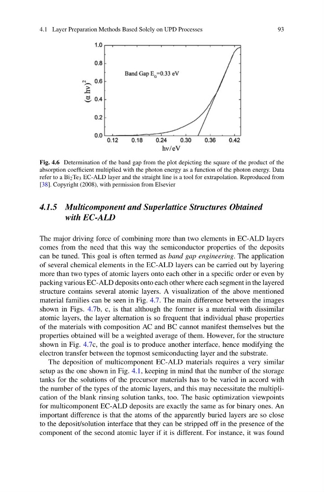
Fig. 4.6 Determination of the band gap from the plot depicting the square of the product of the
absorption coefficient multiplied with the photon energy as a function of the photon energy. Data
refer to a Bi 2 Te 3 EC-ALD layer and the straight line is a tool for extrapolation. Reproduced from
[38]. Copyright (2008), with permission from Elsevier
4.1.5 Multicomponent and Superlattice Structures Obtained
with EC-ALD
The major driving force of combining more than two elements in EC-ALD layers
comes from the need that this way the semiconductor properties of the deposits
can be tuned. This goal is often termed as band gap engineering. The application
of several chemical elements in the EC-ALD layers can be carried out by layering
more than two types of atomic layers onto each other in a specific order or even by
packing various EC-ALD deposits onto each other where each segment in the layered
structure contains several atomic layers. A visualization of the above mentioned
material families can be seen in Fig. 4.7. The main difference between the images
shown in Figs. 4.7b, c, is that although the former is a material with dissimilar
atomic layers, the layer alternation is so frequent that individual phase properties
of the materials with composition AC and BC cannot manifest themselves but the
properties obtained will be a weighted average of them. However, for the structure
shown in Fig. 4.7c, the goal is to produce another interface, hence modifying the
electron transfer between the topmost semiconducting layer and the substrate.
The deposition of multicomponent EC-ALD materials requires a very similar
setup as the one shown in Fig. 4.1, keeping in mind that the number of the storage
tanks for the solutions of the precursor materials has to be varied in accord with
the number of the types of the atomic layers, and this may necessitate the multiplication of the blank rinsing solution tanks, too. The basic optimization viewpoints
for multicomponent EC-ALD deposits are exactly the same as for binary ones. An
important difference is that the atoms of the apparently buried layers are so close
to the deposit/solution interface that they can be stripped off in the presence of the
component of the second atomic layer if it is different. For instance, it was found
93
Fig. 4.6 Determination of the band gap from the plot depicting the square of the product of the
absorption coefficient multiplied with the photon energy as a function of the photon energy. Data
refer to a Bi 2 Te 3 EC-ALD layer and the straight line is a tool for extrapolation. Reproduced from
[38]. Copyright (2008), with permission from Elsevier
4.1.5 Multicomponent and Superlattice Structures Obtained
with EC-ALD
The major driving force of combining more than two elements in EC-ALD layers
comes from the need that this way the semiconductor properties of the deposits
can be tuned. This goal is often termed as band gap engineering. The application
of several chemical elements in the EC-ALD layers can be carried out by layering
more than two types of atomic layers onto each other in a specific order or even by
packing various EC-ALD deposits onto each other where each segment in the layered
structure contains several atomic layers. A visualization of the above mentioned
material families can be seen in Fig. 4.7. The main difference between the images
shown in Figs. 4.7b, c, is that although the former is a material with dissimilar
atomic layers, the layer alternation is so frequent that individual phase properties
of the materials with composition AC and BC cannot manifest themselves but the
properties obtained will be a weighted average of them. However, for the structure
shown in Fig. 4.7c, the goal is to produce another interface, hence modifying the
electron transfer between the topmost semiconducting layer and the substrate.
The deposition of multicomponent EC-ALD materials requires a very similar
setup as the one shown in Fig. 4.1, keeping in mind that the number of the storage
tanks for the solutions of the precursor materials has to be varied in accord with
the number of the types of the atomic layers, and this may necessitate the multiplication of the blank rinsing solution tanks, too. The basic optimization viewpoints
for multicomponent EC-ALD deposits are exactly the same as for binary ones. An
important difference is that the atoms of the apparently buried layers are so close
to the deposit/solution interface that they can be stripped off in the presence of the
component of the second atomic layer if it is different. For instance, it was found