

4.1 Layer Preparation Methods Based Solely on UPD Processes
89
Table 4.1 Summary of the works dealing with EC-ALD of binary compound semiconductors. For
the more electronegative element, the oxidation state of the atoms in the precursor compound is
indicated in parenthesis
S (−2)
As (+3)
Se (+4)
Sb (+3)
Te (+4)
Ni
[20]
Cu
[29]
[49, 50]
Zn
[51]
[52–54]
[55]
Ga
[56]
Mo
[40]
Cd
[9, 24, 51, 57–61]
[9, 27, 42, 62]
[6–10, 15, 30, 63–69]
In
[21, 31]
[34]
[31]
[19]
Sn
[25]
Sb
[22, 36, 37, 70]
Hg
[32, 71]
[72]
Pb
[73]
[35]
[39]
Bi
[23]
[11, 28, 38, 43, 74]
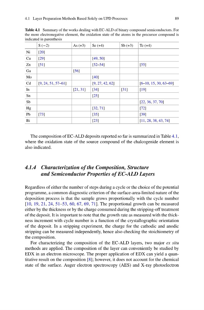
The composition of EC-ALD deposits reported so far is summarized in Table 4.1,
where the oxidation state of the source compound of the chalcogenide element is
also indicated.
4.1.4 Characterization of the Composition, Structure
and Semiconductor Properties of EC-ALD Layers
Regardless of either the number of steps during a cycle or the choice of the potential
programme, a common diagnostic criterion of the surface-area-limited nature of the
deposition process is that the sample grows proportionally with the cycle number
[10, 19, 21, 24, 51–53, 60, 67, 69, 71]. The proportional growth can be measured
either by the thickness or by the charge consumed during the stripping-off treatment
of the deposit. It is important to note that the growth rate as measured with the thickness increment with cycle number is a function of the crystallographic orientation
of the deposit. In a stripping experiment, the charge for the cathodic and anodic
stripping can be measured independently, hence also checking the stoichiometry of
the composition.
For characterizing the composition of the EC-ALD layers, two major ex situ
methods are applied. The composition of the layer can conveniently be studied by
EDX in an electron microscope. The proper application of EDX can yield a quantitative result on the composition [8]; however, it does not account for the chemical
state of the surface. Auger electron spectroscopy (AES) and X-ray photoelectron
89
Table 4.1 Summary of the works dealing with EC-ALD of binary compound semiconductors. For
the more electronegative element, the oxidation state of the atoms in the precursor compound is
indicated in parenthesis
S (−2)
As (+3)
Se (+4)
Sb (+3)
Te (+4)
Ni
[20]
Cu
[29]
[49, 50]
Zn
[51]
[52–54]
[55]
Ga
[56]
Mo
[40]
Cd
[9, 24, 51, 57–61]
[9, 27, 42, 62]
[6–10, 15, 30, 63–69]
In
[21, 31]
[34]
[31]
[19]
Sn
[25]
Sb
[22, 36, 37, 70]
Hg
[32, 71]
[72]
Pb
[73]
[35]
[39]
Bi
[23]
[11, 28, 38, 43, 74]
The composition of EC-ALD deposits reported so far is summarized in Table 4.1,
where the oxidation state of the source compound of the chalcogenide element is
also indicated.
4.1.4 Characterization of the Composition, Structure
and Semiconductor Properties of EC-ALD Layers
Regardless of either the number of steps during a cycle or the choice of the potential
programme, a common diagnostic criterion of the surface-area-limited nature of the
deposition process is that the sample grows proportionally with the cycle number
[10, 19, 21, 24, 51–53, 60, 67, 69, 71]. The proportional growth can be measured
either by the thickness or by the charge consumed during the stripping-off treatment
of the deposit. It is important to note that the growth rate as measured with the thickness increment with cycle number is a function of the crystallographic orientation
of the deposit. In a stripping experiment, the charge for the cathodic and anodic
stripping can be measured independently, hence also checking the stoichiometry of
the composition.
For characterizing the composition of the EC-ALD layers, two major ex situ
methods are applied. The composition of the layer can conveniently be studied by
EDX in an electron microscope. The proper application of EDX can yield a quantitative result on the composition [8]; however, it does not account for the chemical
state of the surface. Auger electron spectroscopy (AES) and X-ray photoelectron