

4.2 Utilizing Electron Emission Spectroscopy
87
25
20
15
10 -5
-10
Normalized intensity
Binding energy (eV)
11.00
9.45 -9.45
26.61
26.79
26.50
26.28
26.17
26.07
26.73
He I
He II
Shift in O 2p
-10 V bias
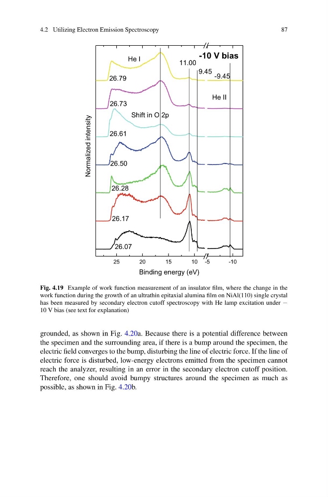
Fig. 4.19 Example of work function measurement of an insulator film, where the change in the
work function during the growth of an ultrathin epitaxial alumina film on NiAl(110) single crystal
has been measured by secondary electron cutoff spectroscopy with He lamp excitation under −
10 V bias (see text for explanation)
grounded, as shown in Fig. 4.20a. Because there is a potential difference between
the specimen and the surrounding area, if there is a bump around the specimen, the
electric field converges to the bump, disturbing the line of electric force. If the line of
electric force is disturbed, low-energy electrons emitted from the specimen cannot
reach the analyzer, resulting in an error in the secondary electron cutoff position.
Therefore, one should avoid bumpy structures around the specimen as much as
possible, as shown in Fig. 4.20b.
87
25
20
15
10 -5
-10
Normalized intensity
Binding energy (eV)
11.00
9.45 -9.45
26.61
26.79
26.50
26.28
26.17
26.07
26.73
He I
He II
Shift in O 2p
-10 V bias
Fig. 4.19 Example of work function measurement of an insulator film, where the change in the
work function during the growth of an ultrathin epitaxial alumina film on NiAl(110) single crystal
has been measured by secondary electron cutoff spectroscopy with He lamp excitation under −
10 V bias (see text for explanation)
grounded, as shown in Fig. 4.20a. Because there is a potential difference between
the specimen and the surrounding area, if there is a bump around the specimen, the
electric field converges to the bump, disturbing the line of electric force. If the line of
electric force is disturbed, low-energy electrons emitted from the specimen cannot
reach the analyzer, resulting in an error in the secondary electron cutoff position.
Therefore, one should avoid bumpy structures around the specimen as much as
possible, as shown in Fig. 4.20b.