

4.2 Utilizing Electron Emission Spectroscopy
81
in air, the surfaces of Pt and Al are not clean, meaning that the obtained values are
different from those in the references.
As expected from the principle in Fig. 4.10, the electrons emitted at the threshold
photon energy (E th ) are those at the lowest binding energy, not those at the Fermi
level, since the electrons are thermally excited near the Fermi level. Therefore, at
high temperatures, the apparent work function obtained from E th in a plot such as
Fig. 4.12 becomes lower. Moreover, from Fig. 4.10, E th corresponds to the ionization
energy (IE) for semiconductors and insulators since the electrons emitted at E th are
those at the lowest binding energy. No electrons are emitted until the photon energy
reaches E th , resulting in much less difficulty in charging with this technique than with
measurement techniques using secondary electron cutoff spectroscopy, as described
in Sect. 4.2.2. The IE of insulators and semiconductors with low carrier density, such
as organic semiconductors, can be measured by PYS. In the case of insulators and
semiconductors, a plot is usually made with the cube root, not the square root, of the
photoelectron emission yield as the ordinate [8, 9], but the assumption of the cube
root is not necessarily realistic. The order of the photoelectron emission yield to be
used is still an open question.
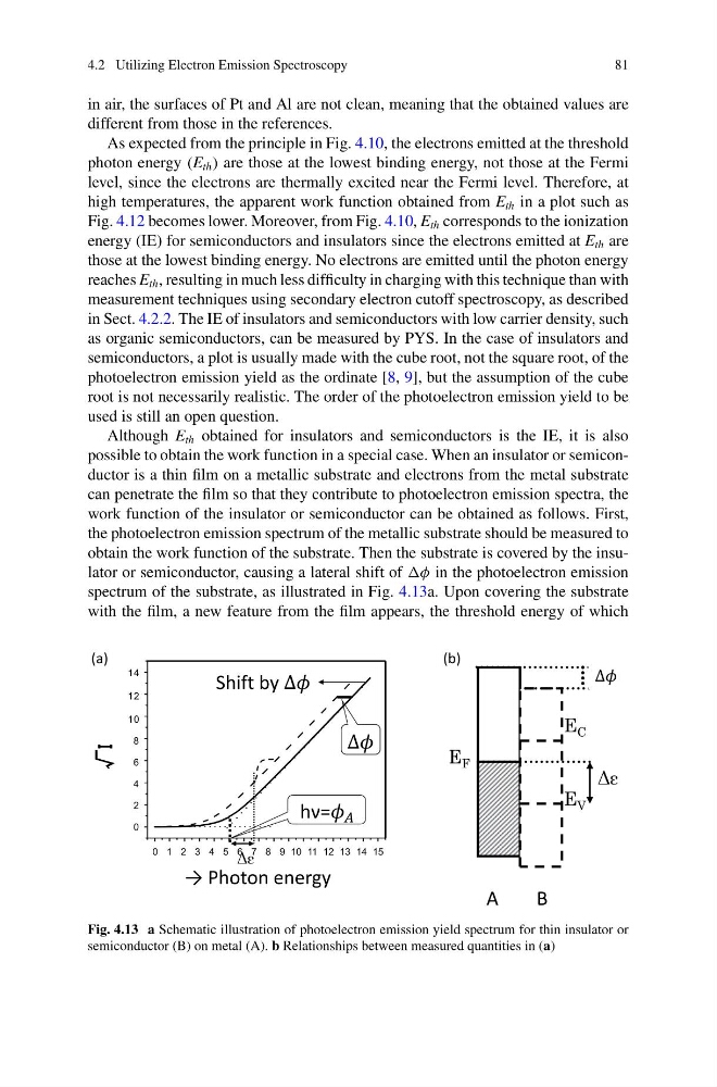
Although E th obtained for insulators and semiconductors is the IE, it is also
possible to obtain the work function in a special case. When an insulator or semiconductor is a thin film on a metallic substrate and electrons from the metal substrate
can penetrate the film so that they contribute to photoelectron emission spectra, the
work function of the insulator or semiconductor can be obtained as follows. First,
the photoelectron emission spectrum of the metallic substrate should be measured to
obtain the work function of the substrate. Then the substrate is covered by the insulator or semiconductor, causing a lateral shift of φ in the photoelectron emission
spectrum of the substrate, as illustrated in Fig. 4.13a. Upon covering the substrate
with the film, a new feature from the film appears, the threshold energy of which
Fig. 4.13 a Schematic illustration of photoelectron emission yield spectrum for thin insulator or
semiconductor (B) on metal (A). b Relationships between measured quantities in (a)
81
in air, the surfaces of Pt and Al are not clean, meaning that the obtained values are
different from those in the references.
As expected from the principle in Fig. 4.10, the electrons emitted at the threshold
photon energy (E th ) are those at the lowest binding energy, not those at the Fermi
level, since the electrons are thermally excited near the Fermi level. Therefore, at
high temperatures, the apparent work function obtained from E th in a plot such as
Fig. 4.12 becomes lower. Moreover, from Fig. 4.10, E th corresponds to the ionization
energy (IE) for semiconductors and insulators since the electrons emitted at E th are
those at the lowest binding energy. No electrons are emitted until the photon energy
reaches E th , resulting in much less difficulty in charging with this technique than with
measurement techniques using secondary electron cutoff spectroscopy, as described
in Sect. 4.2.2. The IE of insulators and semiconductors with low carrier density, such
as organic semiconductors, can be measured by PYS. In the case of insulators and
semiconductors, a plot is usually made with the cube root, not the square root, of the
photoelectron emission yield as the ordinate [8, 9], but the assumption of the cube
root is not necessarily realistic. The order of the photoelectron emission yield to be
used is still an open question.
Although E th obtained for insulators and semiconductors is the IE, it is also
possible to obtain the work function in a special case. When an insulator or semiconductor is a thin film on a metallic substrate and electrons from the metal substrate
can penetrate the film so that they contribute to photoelectron emission spectra, the
work function of the insulator or semiconductor can be obtained as follows. First,
the photoelectron emission spectrum of the metallic substrate should be measured to
obtain the work function of the substrate. Then the substrate is covered by the insulator or semiconductor, causing a lateral shift of φ in the photoelectron emission
spectrum of the substrate, as illustrated in Fig. 4.13a. Upon covering the substrate
with the film, a new feature from the film appears, the threshold energy of which
Fig. 4.13 a Schematic illustration of photoelectron emission yield spectrum for thin insulator or
semiconductor (B) on metal (A). b Relationships between measured quantities in (a)