

6.4 Modification of S Parameter by Inserting Insulator
123
(a)
(b)
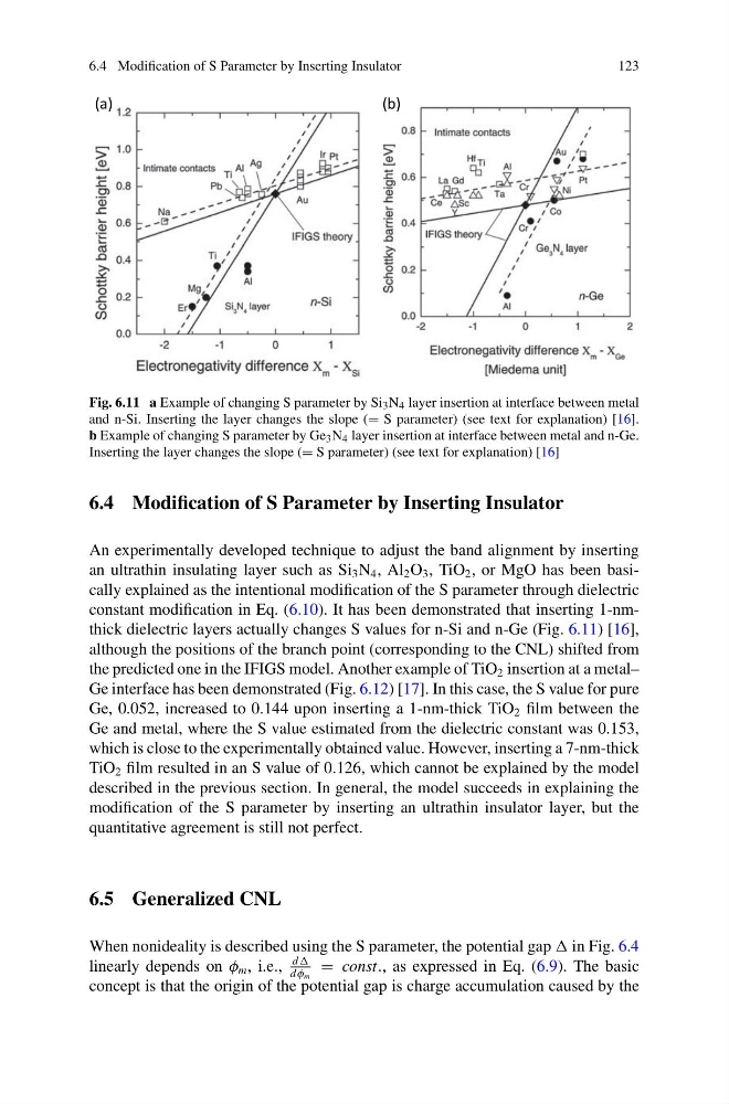
Fig. 6.11 a Example of changing S parameter by Si 3 N 4 layer insertion at interface between metal
and n-Si. Inserting the layer changes the slope (= S parameter) (see text for explanation) [16].
b Example of changing S parameter by Ge 3 N 4 layer insertion at interface between metal and n-Ge.
Inserting the layer changes the slope (= S parameter) (see text for explanation) [16]
6.4 Modification of S Parameter by Inserting Insulator
An experimentally developed technique to adjust the band alignment by inserting
an ultrathin insulating layer such as Si 3 N 4 , Al 2 O 3 , TiO 2 , or MgO has been basically explained as the intentional modification of the S parameter through dielectric
constant modification in Eq. (6.10). It has been demonstrated that inserting 1-nmthick dielectric layers actually changes S values for n-Si and n-Ge (Fig. 6.11) [16],
although the positions of the branch point (corresponding to the CNL) shifted from
the predicted one in the IFIGS model. Another example of TiO 2 insertion at a metal–
Ge interface has been demonstrated (Fig. 6.12) [17]. In this case, the S value for pure
Ge, 0.052, increased to 0.144 upon inserting a 1-nm-thick TiO 2 film between the
Ge and metal, where the S value estimated from the dielectric constant was 0.153,
which is close to the experimentally obtained value. However, inserting a 7-nm-thick
TiO 2 film resulted in an S value of 0.126, which cannot be explained by the model
described in the previous section. In general, the model succeeds in explaining the
modification of the S parameter by inserting an ultrathin insulator layer, but the
quantitative agreement is still not perfect.
6.5 Generalized CNL
When nonideality is described using the S parameter, the potential gap in Fig. 6.4
linearly depends on φ m , i.e.,
d
d φ m
= const., as expressed in Eq. (6.9). The basic
concept is that the origin of the potential gap is charge accumulation caused by the
123
(a)
(b)
Fig. 6.11 a Example of changing S parameter by Si 3 N 4 layer insertion at interface between metal
and n-Si. Inserting the layer changes the slope (= S parameter) (see text for explanation) [16].
b Example of changing S parameter by Ge 3 N 4 layer insertion at interface between metal and n-Ge.
Inserting the layer changes the slope (= S parameter) (see text for explanation) [16]
6.4 Modification of S Parameter by Inserting Insulator
An experimentally developed technique to adjust the band alignment by inserting
an ultrathin insulating layer such as Si 3 N 4 , Al 2 O 3 , TiO 2 , or MgO has been basically explained as the intentional modification of the S parameter through dielectric
constant modification in Eq. (6.10). It has been demonstrated that inserting 1-nmthick dielectric layers actually changes S values for n-Si and n-Ge (Fig. 6.11) [16],
although the positions of the branch point (corresponding to the CNL) shifted from
the predicted one in the IFIGS model. Another example of TiO 2 insertion at a metal–
Ge interface has been demonstrated (Fig. 6.12) [17]. In this case, the S value for pure
Ge, 0.052, increased to 0.144 upon inserting a 1-nm-thick TiO 2 film between the
Ge and metal, where the S value estimated from the dielectric constant was 0.153,
which is close to the experimentally obtained value. However, inserting a 7-nm-thick
TiO 2 film resulted in an S value of 0.126, which cannot be explained by the model
described in the previous section. In general, the model succeeds in explaining the
modification of the S parameter by inserting an ultrathin insulator layer, but the
quantitative agreement is still not perfect.
6.5 Generalized CNL
When nonideality is described using the S parameter, the potential gap in Fig. 6.4
linearly depends on φ m , i.e.,
d
d φ m
= const., as expressed in Eq. (6.9). The basic
concept is that the origin of the potential gap is charge accumulation caused by the