

120
6 Advanced Models for Practical Devices
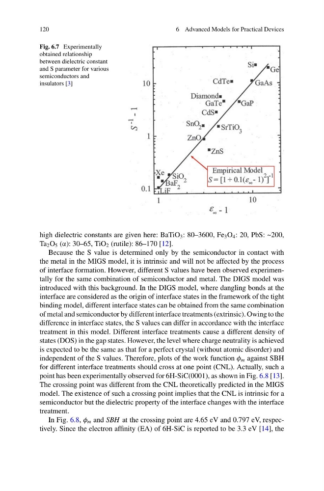
Fig. 6.7 Experimentally
obtained relationship
between dielectric constant
and S parameter for various
semiconductors and
insulators [3]
high dielectric constants are given here: BaTiO 3 : 80–3600, Fe 3 O 4 : 20, PbS: ~200,
Ta 2 O 5 (α): 30–65, TiO 2 (rutile): 86–170 [12].
Because the S value is determined only by the semiconductor in contact with
the metal in the MIGS model, it is intrinsic and will not be affected by the process
of interface formation. However, different S values have been observed experimentally for the same combination of semiconductor and metal. The DIGS model was
introduced with this background. In the DIGS model, where dangling bonds at the
interface are considered as the origin of interface states in the framework of the tight
binding model, different interface states can be obtained from the same combination
of metal and semiconductor by different interface treatments (extrinsic). Owing to the
difference in interface states, the S values can differ in accordance with the interface
treatment in this model. Different interface treatments cause a different density of
states (DOS) in the gap states. However, the level where charge neutrality is achieved
is expected to be the same as that for a perfect crystal (without atomic disorder) and
independent of the S values. Therefore, plots of the work function φ m against SBH
for different interface treatments should cross at one point (CNL). Actually, such a
point has been experimentally observed for 6H-SiC(0001), as shown in Fig. 6.8 [13].
The crossing point was different from the CNL theoretically predicted in the MIGS
model. The existence of such a crossing point implies that the CNL is intrinsic for a
semiconductor but the dielectric property of the interface changes with the interface
treatment.
In Fig. 6.8, φ m and SBH at the crossing point are 4.65 eV and 0.797 eV, respectively. Since the electron affinity (EA) of 6H-SiC is reported to be 3.3 eV [14], the
6 Advanced Models for Practical Devices
Fig. 6.7 Experimentally
obtained relationship
between dielectric constant
and S parameter for various
semiconductors and
insulators [3]
high dielectric constants are given here: BaTiO 3 : 80–3600, Fe 3 O 4 : 20, PbS: ~200,
Ta 2 O 5 (α): 30–65, TiO 2 (rutile): 86–170 [12].
Because the S value is determined only by the semiconductor in contact with
the metal in the MIGS model, it is intrinsic and will not be affected by the process
of interface formation. However, different S values have been observed experimentally for the same combination of semiconductor and metal. The DIGS model was
introduced with this background. In the DIGS model, where dangling bonds at the
interface are considered as the origin of interface states in the framework of the tight
binding model, different interface states can be obtained from the same combination
of metal and semiconductor by different interface treatments (extrinsic). Owing to the
difference in interface states, the S values can differ in accordance with the interface
treatment in this model. Different interface treatments cause a different density of
states (DOS) in the gap states. However, the level where charge neutrality is achieved
is expected to be the same as that for a perfect crystal (without atomic disorder) and
independent of the S values. Therefore, plots of the work function φ m against SBH
for different interface treatments should cross at one point (CNL). Actually, such a
point has been experimentally observed for 6H-SiC(0001), as shown in Fig. 6.8 [13].
The crossing point was different from the CNL theoretically predicted in the MIGS
model. The existence of such a crossing point implies that the CNL is intrinsic for a
semiconductor but the dielectric property of the interface changes with the interface
treatment.
In Fig. 6.8, φ m and SBH at the crossing point are 4.65 eV and 0.797 eV, respectively. Since the electron affinity (EA) of 6H-SiC is reported to be 3.3 eV [14], the