

5.2 Modification of Band Alignment
107
Metal A
Metal B
Band diagram of interface between
metal A and n-semiconductor
Band diagram of interface with inserron
of interface layer of metal B
E VAC
E C
E V
E F
E F
E VAC
EA
SBH
E F
E VAC
E VAC
E VAC
E C
E V
E F
EA
SBH
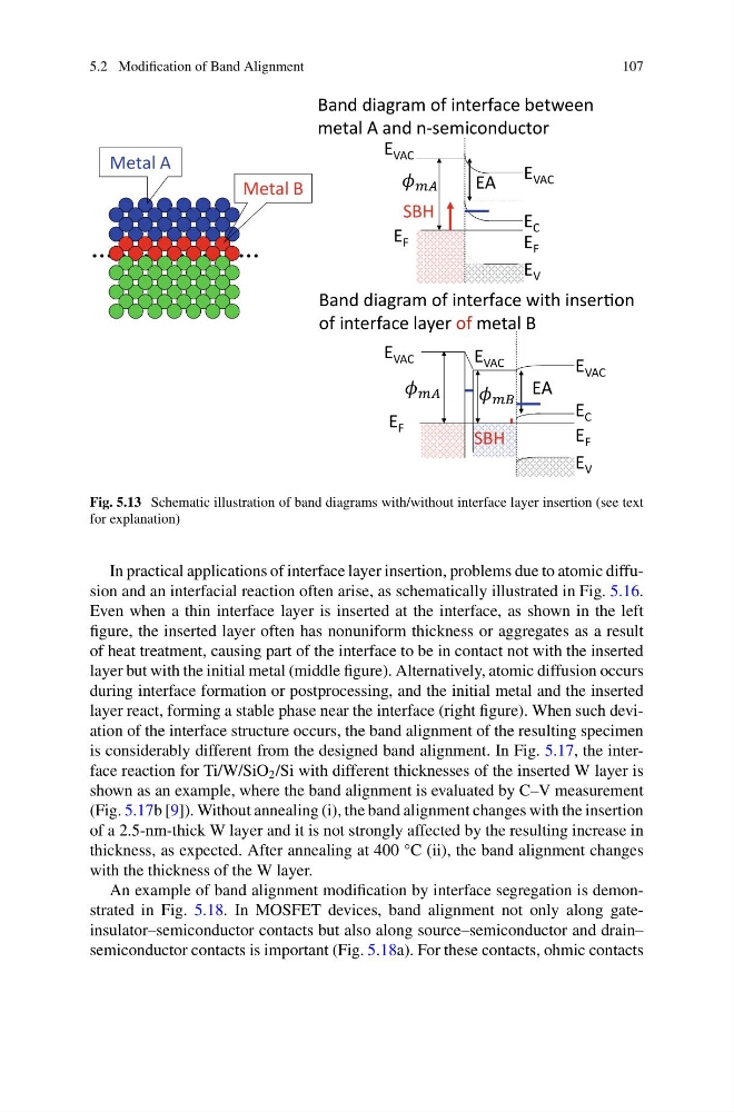
Fig. 5.13 Schematic illustration of band diagrams with/without interface layer insertion (see text
for explanation)
In practical applications of interface layer insertion, problems due to atomic diffusion and an interfacial reaction often arise, as schematically illustrated in Fig. 5.16.
Even when a thin interface layer is inserted at the interface, as shown in the left
figure, the inserted layer often has nonuniform thickness or aggregates as a result
of heat treatment, causing part of the interface to be in contact not with the inserted
layer but with the initial metal (middle figure). Alternatively, atomic diffusion occurs
during interface formation or postprocessing, and the initial metal and the inserted
layer react, forming a stable phase near the interface (right figure). When such deviation of the interface structure occurs, the band alignment of the resulting specimen
is considerably different from the designed band alignment. In Fig. 5.17, the interface reaction for Ti/W/SiO 2 /Si with different thicknesses of the inserted W layer is
shown as an example, where the band alignment is evaluated by C–V measurement
(Fig. 5.17b [9]). Without annealing (i), the band alignment changes with the insertion
of a 2.5-nm-thick W layer and it is not strongly affected by the resulting increase in
thickness, as expected. After annealing at 400 °C (ii), the band alignment changes
with the thickness of the W layer.
An example of band alignment modification by interface segregation is demonstrated in Fig. 5.18. In MOSFET devices, band alignment not only along gateinsulator–semiconductor contacts but also along source–semiconductor and drain–
semiconductor contacts is important (Fig. 5.18a). For these contacts, ohmic contacts
107
Metal A
Metal B
Band diagram of interface between
metal A and n-semiconductor
Band diagram of interface with inserron
of interface layer of metal B
E VAC
E C
E V
E F
E F
E VAC
EA
SBH
E F
E VAC
E VAC
E VAC
E C
E V
E F
EA
SBH
Fig. 5.13 Schematic illustration of band diagrams with/without interface layer insertion (see text
for explanation)
In practical applications of interface layer insertion, problems due to atomic diffusion and an interfacial reaction often arise, as schematically illustrated in Fig. 5.16.
Even when a thin interface layer is inserted at the interface, as shown in the left
figure, the inserted layer often has nonuniform thickness or aggregates as a result
of heat treatment, causing part of the interface to be in contact not with the inserted
layer but with the initial metal (middle figure). Alternatively, atomic diffusion occurs
during interface formation or postprocessing, and the initial metal and the inserted
layer react, forming a stable phase near the interface (right figure). When such deviation of the interface structure occurs, the band alignment of the resulting specimen
is considerably different from the designed band alignment. In Fig. 5.17, the interface reaction for Ti/W/SiO 2 /Si with different thicknesses of the inserted W layer is
shown as an example, where the band alignment is evaluated by C–V measurement
(Fig. 5.17b [9]). Without annealing (i), the band alignment changes with the insertion
of a 2.5-nm-thick W layer and it is not strongly affected by the resulting increase in
thickness, as expected. After annealing at 400 °C (ii), the band alignment changes
with the thickness of the W layer.
An example of band alignment modification by interface segregation is demonstrated in Fig. 5.18. In MOSFET devices, band alignment not only along gateinsulator–semiconductor contacts but also along source–semiconductor and drain–
semiconductor contacts is important (Fig. 5.18a). For these contacts, ohmic contacts