

5.2 Modification of Band Alignment
105
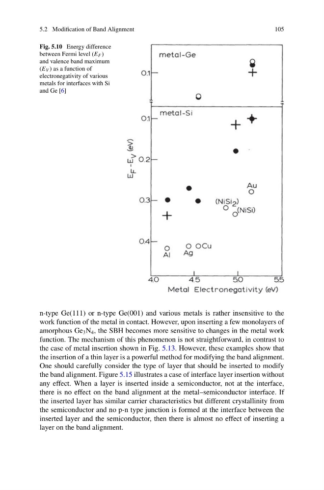
Fig. 5.10 Energy difference
between Fermi level (E F )
and valence band maximum
(E V ) as a function of
electronegativity of various
metals for interfaces with Si
and Ge [6]
n-type Ge(111) or n-type Ge(001) and various metals is rather insensitive to the
work function of the metal in contact. However, upon inserting a few monolayers of
amorphous Ge 3 N 4 , the SBH becomes more sensitive to changes in the metal work
function. The mechanism of this phenomenon is not straightforward, in contrast to
the case of metal insertion shown in Fig. 5.13. However, these examples show that
the insertion of a thin layer is a powerful method for modifying the band alignment.
One should carefully consider the type of layer that should be inserted to modify
the band alignment. Figure 5.15 illustrates a case of interface layer insertion without
any effect. When a layer is inserted inside a semiconductor, not at the interface,
there is no effect on the band alignment at the metal–semiconductor interface. If
the inserted layer has similar carrier characteristics but different crystallinity from
the semiconductor and no p-n type junction is formed at the interface between the
inserted layer and the semiconductor, then there is almost no effect of inserting a
layer on the band alignment.
105
Fig. 5.10 Energy difference
between Fermi level (E F )
and valence band maximum
(E V ) as a function of
electronegativity of various
metals for interfaces with Si
and Ge [6]
n-type Ge(111) or n-type Ge(001) and various metals is rather insensitive to the
work function of the metal in contact. However, upon inserting a few monolayers of
amorphous Ge 3 N 4 , the SBH becomes more sensitive to changes in the metal work
function. The mechanism of this phenomenon is not straightforward, in contrast to
the case of metal insertion shown in Fig. 5.13. However, these examples show that
the insertion of a thin layer is a powerful method for modifying the band alignment.
One should carefully consider the type of layer that should be inserted to modify
the band alignment. Figure 5.15 illustrates a case of interface layer insertion without
any effect. When a layer is inserted inside a semiconductor, not at the interface,
there is no effect on the band alignment at the metal–semiconductor interface. If
the inserted layer has similar carrier characteristics but different crystallinity from
the semiconductor and no p-n type junction is formed at the interface between the
inserted layer and the semiconductor, then there is almost no effect of inserting a
layer on the band alignment.