

98
5 Modification of Band Alignment via Work Function Control
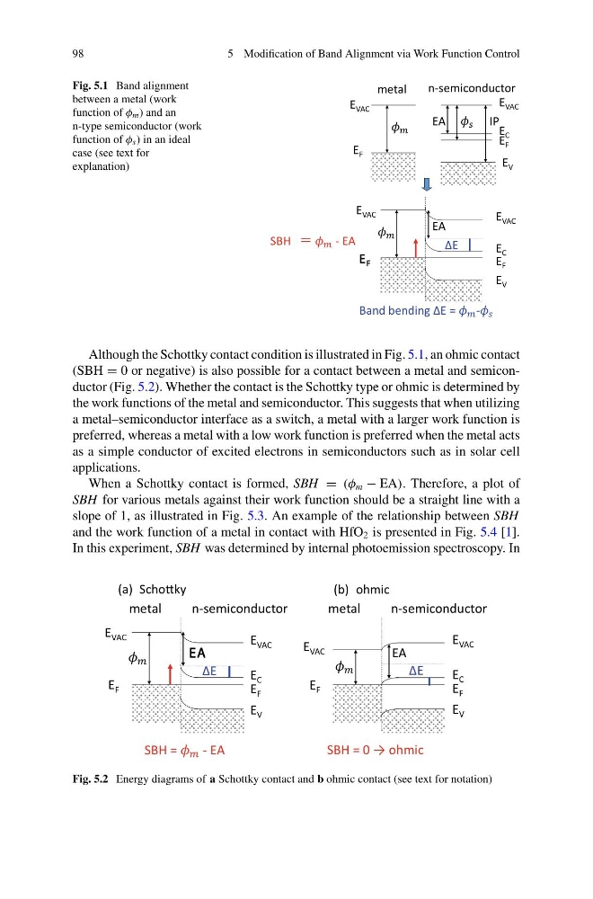
Fig. 5.1 Band alignment
between a metal (work
function of φ m ) and an
n-type semiconductor (work
function of φ s ) in an ideal
case (see text for
explanation)
E F
metal
E VAC
n-semiconductor
E VAC
E C
E V
E F
EA
IP
SBH
- EA
Band bending ΔE =
-
E VAC
E C
E V
E F
E VAC
EA
ΔE
Although the Schottky contact condition is illustrated in Fig. 5.1, an ohmic contact
(SBH = 0 or negative) is also possible for a contact between a metal and semiconductor (Fig. 5.2). Whether the contact is the Schottky type or ohmic is determined by
the work functions of the metal and semiconductor. This suggests that when utilizing
a metal–semiconductor interface as a switch, a metal with a larger work function is
preferred, whereas a metal with a low work function is preferred when the metal acts
as a simple conductor of excited electrons in semiconductors such as in solar cell
applications.
When a Schottky contact is formed, SBH = (φ m − EA). Therefore, a plot of
SBH for various metals against their work function should be a straight line with a
slope of 1, as illustrated in Fig. 5.3. An example of the relationship between SBH
and the work function of a metal in contact with HfO 2 is presented in Fig. 5.4 [1].
In this experiment, SBH was determined by internal photoemission spectroscopy. In
E VAC
E C
E V
E F
E F
E VAC
ΔE
SBH =
- EA
E VAC
E C
E V
E F
E F
E VAC
EA
ΔE
(a) SchoƩky
(b) ohmic
metal
n-semiconductor
SBH = 0 → ohmic
metal
n-semiconductor
Fig. 5.2 Energy diagrams of a Schottky contact and b ohmic contact (see text for notation)
5 Modification of Band Alignment via Work Function Control
Fig. 5.1 Band alignment
between a metal (work
function of φ m ) and an
n-type semiconductor (work
function of φ s ) in an ideal
case (see text for
explanation)
E F
metal
E VAC
n-semiconductor
E VAC
E C
E V
E F
EA
IP
SBH
- EA
Band bending ΔE =
-
E VAC
E C
E V
E F
E VAC
EA
ΔE
Although the Schottky contact condition is illustrated in Fig. 5.1, an ohmic contact
(SBH = 0 or negative) is also possible for a contact between a metal and semiconductor (Fig. 5.2). Whether the contact is the Schottky type or ohmic is determined by
the work functions of the metal and semiconductor. This suggests that when utilizing
a metal–semiconductor interface as a switch, a metal with a larger work function is
preferred, whereas a metal with a low work function is preferred when the metal acts
as a simple conductor of excited electrons in semiconductors such as in solar cell
applications.
When a Schottky contact is formed, SBH = (φ m − EA). Therefore, a plot of
SBH for various metals against their work function should be a straight line with a
slope of 1, as illustrated in Fig. 5.3. An example of the relationship between SBH
and the work function of a metal in contact with HfO 2 is presented in Fig. 5.4 [1].
In this experiment, SBH was determined by internal photoemission spectroscopy. In
E VAC
E C
E V
E F
E F
E VAC
ΔE
SBH =
- EA
E VAC
E C
E V
E F
E F
E VAC
EA
ΔE
(a) SchoƩky
(b) ohmic
metal
n-semiconductor
SBH = 0 → ohmic
metal
n-semiconductor
Fig. 5.2 Energy diagrams of a Schottky contact and b ohmic contact (see text for notation)