

3 Percolation Toward Lateral Junctions
67
3.4.5 Lateral Alternating Multilayered Junction
The hole range (L h = 0.4 mm) and the electron range (L e = 0.2 mm) were determined.
Thus, we adjusted the width of the overlap between C8-BTBT and PTCDI-C8 in
the lateral alternating multilayered junction to less than 0.4 mm and 0.2 mm, i.e.,
0.14 mm for the total extractions of holes and electrons to the respective electrode
(Fig. 3.15a). The hole and electron pathways were selectively connected to only
the hole- and electron-collecting electrodes, respectively (Fig. 3.15a), by using a
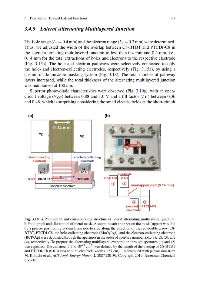
custom-made movable masking system (Fig. 3.18). The total number of pathway
layers increased, while the total thickness of the alternating multilayered junction
was maintained at 100 nm.
Superior photovoltaic characteristics were observed (Fig. 3.19a), with an opencircuit voltage (V OC ) between 0.88 and 1.0 V and a fill factor (FF) between 0.36
and 0.48, which is surprising considering the small electric fields at the short-circuit
overlapped part (0.14 mm)
C8-BTBT
electrode
(hole)
electrode
(electron)
PTCDI-C8
Ag
Ag
0.14 mm
50 nm
PTCDI-C8
C8-BTBT
h +
e -
Ag
MoO 3
Ag
BCP
(a)
(b)
hole collecting
electrode
electron collecting
electrode
sapphire substrate
Fig. 3.18 a Photograph and corresponding structure of lateral alternating multilayered junction.
b Photograph and illustration of metal mask. A sapphire substrate set on the mask (upper) was slid
by a precise positioning system from side to side along the direction of the red double arrow. C8BTBT, PTCDI-C8, the hole-collecting electrode (MoO 3 /Ag), and the electron-collecting electrode
(BCP/Ag) were deposited through the apertures in the order of aperture number, i.e., (1), (2), (3), and
(4), respectively. To prepare the alternating multilayers, evaporation through apertures (1) and (2)
was repeated. The cell area (7.7 × 10 −3 cm 2 ) was defined by the length of the overlap of C8-BTBT
and PTCDI-C8 (0.014 cm) and the electrode width (0.57 cm). Reproduced with permission from
M. Kikuchi et al., ACS Appl. Energy Mater., 2, 2087 (2019). Copyright 2019, American Chemical
Society
67
3.4.5 Lateral Alternating Multilayered Junction
The hole range (L h = 0.4 mm) and the electron range (L e = 0.2 mm) were determined.
Thus, we adjusted the width of the overlap between C8-BTBT and PTCDI-C8 in
the lateral alternating multilayered junction to less than 0.4 mm and 0.2 mm, i.e.,
0.14 mm for the total extractions of holes and electrons to the respective electrode
(Fig. 3.15a). The hole and electron pathways were selectively connected to only
the hole- and electron-collecting electrodes, respectively (Fig. 3.15a), by using a
custom-made movable masking system (Fig. 3.18). The total number of pathway
layers increased, while the total thickness of the alternating multilayered junction
was maintained at 100 nm.
Superior photovoltaic characteristics were observed (Fig. 3.19a), with an opencircuit voltage (V OC ) between 0.88 and 1.0 V and a fill factor (FF) between 0.36
and 0.48, which is surprising considering the small electric fields at the short-circuit
overlapped part (0.14 mm)
C8-BTBT
electrode
(hole)
electrode
(electron)
PTCDI-C8
Ag
Ag
0.14 mm
50 nm
PTCDI-C8
C8-BTBT
h +
e -
Ag
MoO 3
Ag
BCP
(a)
(b)
hole collecting
electrode
electron collecting
electrode
sapphire substrate
Fig. 3.18 a Photograph and corresponding structure of lateral alternating multilayered junction.
b Photograph and illustration of metal mask. A sapphire substrate set on the mask (upper) was slid
by a precise positioning system from side to side along the direction of the red double arrow. C8BTBT, PTCDI-C8, the hole-collecting electrode (MoO 3 /Ag), and the electron-collecting electrode
(BCP/Ag) were deposited through the apertures in the order of aperture number, i.e., (1), (2), (3), and
(4), respectively. To prepare the alternating multilayers, evaporation through apertures (1) and (2)
was repeated. The cell area (7.7 × 10 −3 cm 2 ) was defined by the length of the overlap of C8-BTBT
and PTCDI-C8 (0.014 cm) and the electrode width (0.57 cm). Reproduced with permission from
M. Kikuchi et al., ACS Appl. Energy Mater., 2, 2087 (2019). Copyright 2019, American Chemical
Society