

66
M. Hiramoto
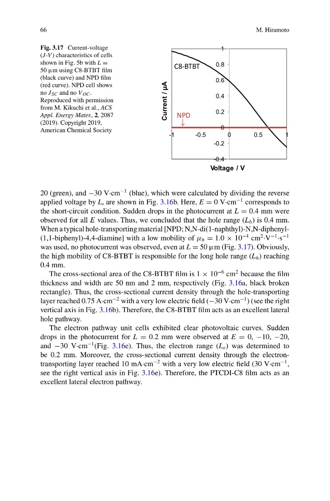
Fig. 3.17 Current-voltage
(J-V ) characteristics of cells
shown in Fig. 5b with L =
50 μm using C8-BTBT film
(black curve) and NPD film
(red curve). NPD cell shows
no J SC and no V OC .
Reproduced with permission
from M. Kikuchi et al., ACS
Appl. Energy Mater., 2, 2087
(2019). Copyright 2019,
American Chemical Society
-0.4
-0.2
0
0.2
0.4
0.6
0.8
1
-1
-0.5
0
0.5
1
C8-BTBT
NPD
Current / µA
Voltage / V
20 (green), and −30 V·cm
−1 (blue), which were calculated by dividing the reverse
applied voltage by L, are shown in Fig. 3.16b. Here, E = 0 V·cm
−1 corresponds to
the short-circuit condition. Sudden drops in the photocurrent at L = 0.4 mm were
observed for all E values. Thus, we concluded that the hole range (L h ) is 0.4 mm.
When a typical hole-transporting material [NPD; N,N-di(1-naphthyl)-N,N-diphenyl(1,1-biphenyl)-4,4-diamine] with a low mobility of μ h = 1.0 × 10
−4 cm
2 ·V
−1 ·s
−1
was used, no photocurrent was observed, even at L = 50 μm (Fig. 3.17). Obviously,
the high mobility of C8-BTBT is responsible for the long hole range (L h ) reaching
0.4 mm.
The cross-sectional area of the C8-BTBT film is 1 × 10
−6 cm
2 because the film
thickness and width are 50 nm and 2 mm, respectively (Fig. 3.16a, black broken
rectangle). Thus, the cross-sectional current density through the hole-transporting
layer reached 0.75 A·cm
−2 with a very low electric field (−30 V·cm
−1 ) (see the right
vertical axis in Fig. 3.16b). Therefore, the C8-BTBT film acts as an excellent lateral
hole pathway.
The electron pathway unit cells exhibited clear photovoltaic curves. Sudden
drops in the photocurrent for L = 0.2 mm were observed at E = 0, −10, −20,
and −30 V·cm
−1 (Fig. 3.16e). Thus, the electron range (L e ) was determined to
be 0.2 mm. Moreover, the cross-sectional current density through the electrontransporting layer reached 10 mA·cm
−2 with a very low electric field (30 V·cm
−1 ,
see the right vertical axis in Fig. 3.16e). Therefore, the PTCDI-C8 film acts as an
excellent lateral electron pathway.
M. Hiramoto
Fig. 3.17 Current-voltage
(J-V ) characteristics of cells
shown in Fig. 5b with L =
50 μm using C8-BTBT film
(black curve) and NPD film
(red curve). NPD cell shows
no J SC and no V OC .
Reproduced with permission
from M. Kikuchi et al., ACS
Appl. Energy Mater., 2, 2087
(2019). Copyright 2019,
American Chemical Society
-0.4
-0.2
0
0.2
0.4
0.6
0.8
1
-1
-0.5
0
0.5
1
C8-BTBT
NPD
Current / µA
Voltage / V
20 (green), and −30 V·cm
−1 (blue), which were calculated by dividing the reverse
applied voltage by L, are shown in Fig. 3.16b. Here, E = 0 V·cm
−1 corresponds to
the short-circuit condition. Sudden drops in the photocurrent at L = 0.4 mm were
observed for all E values. Thus, we concluded that the hole range (L h ) is 0.4 mm.
When a typical hole-transporting material [NPD; N,N-di(1-naphthyl)-N,N-diphenyl(1,1-biphenyl)-4,4-diamine] with a low mobility of μ h = 1.0 × 10
−4 cm
2 ·V
−1 ·s
−1
was used, no photocurrent was observed, even at L = 50 μm (Fig. 3.17). Obviously,
the high mobility of C8-BTBT is responsible for the long hole range (L h ) reaching
0.4 mm.
The cross-sectional area of the C8-BTBT film is 1 × 10
−6 cm
2 because the film
thickness and width are 50 nm and 2 mm, respectively (Fig. 3.16a, black broken
rectangle). Thus, the cross-sectional current density through the hole-transporting
layer reached 0.75 A·cm
−2 with a very low electric field (−30 V·cm
−1 ) (see the right
vertical axis in Fig. 3.16b). Therefore, the C8-BTBT film acts as an excellent lateral
hole pathway.
The electron pathway unit cells exhibited clear photovoltaic curves. Sudden
drops in the photocurrent for L = 0.2 mm were observed at E = 0, −10, −20,
and −30 V·cm
−1 (Fig. 3.16e). Thus, the electron range (L e ) was determined to
be 0.2 mm. Moreover, the cross-sectional current density through the electrontransporting layer reached 10 mA·cm
−2 with a very low electric field (30 V·cm
−1 ,
see the right vertical axis in Fig. 3.16e). Therefore, the PTCDI-C8 film acts as an
excellent lateral electron pathway.