

64
M. Hiramoto
mobility has been observed in the direction parallel to the substrate owing to strong
π-π interactions (Fig. 3.15), this concept is suitable for the lateral device.
(d)
Electron Collecting
Electrode
(BCP/Ag)
H 2 Pc
(50 nm)
Hole Collecting
Electrode
(MoO 3 /Ag)
Sapphire substrate
h +
L e = 0.2 mm
0.1
0.2
0.3
0.4
Current / µA
1
Cross-sectional
current density / mA cm -2
0
0.001
— 0 V/cm
— 10 V/cm
— 20 V/cm
— 30 V/cm
PTCDI-C8
e -
0.005
10
5
A
B
C
Cross-sectional area
(50 nm
2 mm)
Inter electrode distance (L)
0.05 –0.4 mm
L / mm
L h = 0.4 mm
e -
Electron Collecting
Electrode
(BCP/Ag)
C 60
(50 nm)
Hole Collecting
Electrode
(MoO 3 /Ag)
Sapphire substrate
h
0.01
0.1
1
— 0 V/cm
— 10 V/cm
— 20 V/cm
— 30 V/cm
100
10
1000
Cross-sectional
current density / mA cm -2
0.1
0.2
0.3
0.4
0.5
0.6
0.7
Current / µA
(a)
(c)
-1
-0.5
0
0.5
1
1.5
Voltage / V
1.0
0.8
0.6
0.4
0.2
-0.2
-0.4
L=0.05 mm
0.10 mm
0.20 mm
0.40 mm
0.50 mm
0.60 mm
Current / µA
(b)
A
B
C
h+
(50 nm
2 mm)
Inter electrode distance(L)
0.05 –0.6 mm
0
L / mm
Starting line
Starting line
0
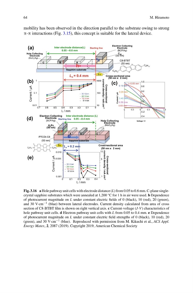
Fig. 3.16 a Hole pathway unit cells with electrode distance (L) from 0.05 to 0.6 mm. C-plane singlecrystal sapphire substrates which were annealed at 1,200 °C for 1 h in air were used. b Dependence
of photocurrent magnitude on L under constant electric fields of 0 (black), 10 (red), 20 (green),
and 30 V·cm −1 (blue) between lateral electrodes. Current density calculated from area of cross
section of C8-BTBT film is shown on right vertical axis. c Current-voltage (J-V ) characteristics of
hole pathway unit cells. d Electron pathway unit cells with L from 0.05 to 0.4 mm. e Dependence
of photocurrent magnitude on L under constant electric field strengths of 0 (black), 10 (red), 20
(green), and 30 V·cm −1 (blue). Reproduced with permission from M. Kikuchi et al., ACS Appl.
Energy Mater., 2, 2087 (2019). Copyright 2019, American Chemical Society
M. Hiramoto
mobility has been observed in the direction parallel to the substrate owing to strong
π-π interactions (Fig. 3.15), this concept is suitable for the lateral device.
(d)
Electron Collecting
Electrode
(BCP/Ag)
H 2 Pc
(50 nm)
Hole Collecting
Electrode
(MoO 3 /Ag)
Sapphire substrate
h +
L e = 0.2 mm
0.1
0.2
0.3
0.4
Current / µA
1
Cross-sectional
current density / mA cm -2
0
0.001
— 0 V/cm
— 10 V/cm
— 20 V/cm
— 30 V/cm
PTCDI-C8
e -
0.005
10
5
A
B
C
Cross-sectional area
(50 nm
2 mm)
Inter electrode distance (L)
0.05 –0.4 mm
L / mm
L h = 0.4 mm
e -
Electron Collecting
Electrode
(BCP/Ag)
C 60
(50 nm)
Hole Collecting
Electrode
(MoO 3 /Ag)
Sapphire substrate
h
0.01
0.1
1
— 0 V/cm
— 10 V/cm
— 20 V/cm
— 30 V/cm
100
10
1000
Cross-sectional
current density / mA cm -2
0.1
0.2
0.3
0.4
0.5
0.6
0.7
Current / µA
(a)
(c)
-1
-0.5
0
0.5
1
1.5
Voltage / V
1.0
0.8
0.6
0.4
0.2
-0.2
-0.4
L=0.05 mm
0.10 mm
0.20 mm
0.40 mm
0.50 mm
0.60 mm
Current / µA
(b)
A
B
C
h+
(50 nm
2 mm)
Inter electrode distance(L)
0.05 –0.6 mm
0
L / mm
Starting line
Starting line
0
Fig. 3.16 a Hole pathway unit cells with electrode distance (L) from 0.05 to 0.6 mm. C-plane singlecrystal sapphire substrates which were annealed at 1,200 °C for 1 h in air were used. b Dependence
of photocurrent magnitude on L under constant electric fields of 0 (black), 10 (red), 20 (green),
and 30 V·cm −1 (blue) between lateral electrodes. Current density calculated from area of cross
section of C8-BTBT film is shown on right vertical axis. c Current-voltage (J-V ) characteristics of
hole pathway unit cells. d Electron pathway unit cells with L from 0.05 to 0.4 mm. e Dependence
of photocurrent magnitude on L under constant electric field strengths of 0 (black), 10 (red), 20
(green), and 30 V·cm −1 (blue). Reproduced with permission from M. Kikuchi et al., ACS Appl.
Energy Mater., 2, 2087 (2019). Copyright 2019, American Chemical Society