

3 Percolation Toward Lateral Junctions
63
Electrode
e
-
h +
(a)
h
Electrode
0.14 mm
10 nm
Sapphire
Substrate
(c)
(b)
h +
e
-
+
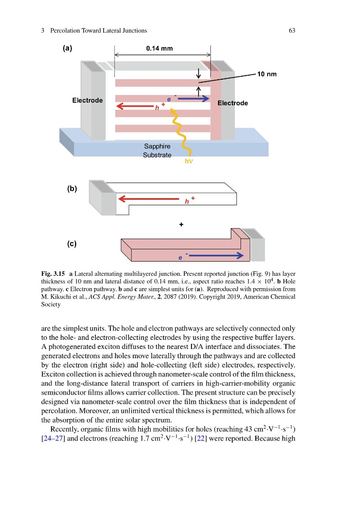
Fig. 3.15 a Lateral alternating multilayered junction. Present reported junction (Fig. 9) has layer
thickness of 10 nm and lateral distance of 0.14 mm, i.e., aspect ratio reaches 1.4 × 10 4 . b Hole
pathway. c Electron pathway. b and c are simplest units for (a). Reproduced with permission from
M. Kikuchi et al., ACS Appl. Energy Mater., 2, 2087 (2019). Copyright 2019, American Chemical
Society
are the simplest units. The hole and electron pathways are selectively connected only
to the hole- and electron-collecting electrodes by using the respective buffer layers.
A photogenerated exciton diffuses to the nearest D/A interface and dissociates. The
generated electrons and holes move laterally through the pathways and are collected
by the electron (right side) and hole-collecting (left side) electrodes, respectively.
Exciton collection is achieved through nanometer-scale control of the film thickness,
and the long-distance lateral transport of carriers in high-carrier-mobility organic
semiconductor films allows carrier collection. The present structure can be precisely
designed via nanometer-scale control over the film thickness that is independent of
percolation. Moreover, an unlimited vertical thickness is permitted, which allows for
the absorption of the entire solar spectrum.
Recently, organic films with high mobilities for holes (reaching 43 cm
2 ·V
−1 ·s
−1 )
[24–27] and electrons (reaching 1.7 cm
2 ·V
−1 ·s
−1 ) [22] were reported. Because high
63
Electrode
e
-
h +
(a)
h
Electrode
0.14 mm
10 nm
Sapphire
Substrate
(c)
(b)
h +
e
-
+
Fig. 3.15 a Lateral alternating multilayered junction. Present reported junction (Fig. 9) has layer
thickness of 10 nm and lateral distance of 0.14 mm, i.e., aspect ratio reaches 1.4 × 10 4 . b Hole
pathway. c Electron pathway. b and c are simplest units for (a). Reproduced with permission from
M. Kikuchi et al., ACS Appl. Energy Mater., 2, 2087 (2019). Copyright 2019, American Chemical
Society
are the simplest units. The hole and electron pathways are selectively connected only
to the hole- and electron-collecting electrodes by using the respective buffer layers.
A photogenerated exciton diffuses to the nearest D/A interface and dissociates. The
generated electrons and holes move laterally through the pathways and are collected
by the electron (right side) and hole-collecting (left side) electrodes, respectively.
Exciton collection is achieved through nanometer-scale control of the film thickness,
and the long-distance lateral transport of carriers in high-carrier-mobility organic
semiconductor films allows carrier collection. The present structure can be precisely
designed via nanometer-scale control over the film thickness that is independent of
percolation. Moreover, an unlimited vertical thickness is permitted, which allows for
the absorption of the entire solar spectrum.
Recently, organic films with high mobilities for holes (reaching 43 cm
2 ·V
−1 ·s
−1 )
[24–27] and electrons (reaching 1.7 cm
2 ·V
−1 ·s
−1 ) [22] were reported. Because high