

3 Percolation Toward Lateral Junctions
55
0.01
0.1
1
1
10
100
Layer width (x) / nm
5
x = 5 nm
Active area
(a)
(b)
C 60 /H 2 Pc
heterojunction
h
Active area
Active area
H 2 Pc/C 60
heterojunction
h +
e -
h +
e -
e -
h +
Dead area
Exciton
(c)
0.01
.
0.1
1
0
20
40
60
80
100
Layer width (x) / nm
(d)
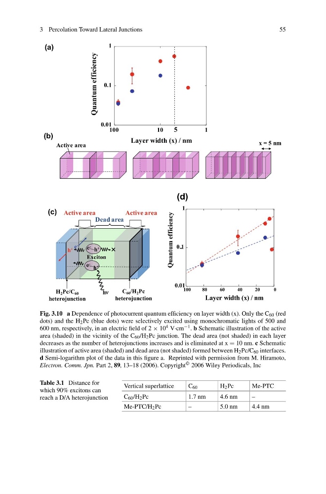
Fig. 3.10 a Dependence of photocurrent quantum efficiency on layer width (x). Only the C 60 (red
dots) and the H 2 Pc (blue dots) were selectively excited using monochromatic lights of 500 and
600 nm, respectively, in an electric field of 2 × 10 4 V·cm −1 . b Schematic illustration of the active
area (shaded) in the vicinity of the C 60 /H 2 Pc junction. The dead area (not shaded) in each layer
decreases as the number of heterojunctions increases and is eliminated at x = 10 nm. c Schematic
illustration of active area (shaded) and dead area (not shaded) formed between H 2 Pc/C 60 interfaces.
d Semi-logarithm plot of the data in this figure a. Reprinted with permission from M. Hiramoto,
Electron. Comm. Jpn. Part 2, 89, 13–18 (2006). Copyright © 2006 Wiley Periodicals, Inc
Table 3.1 Distance for
which 90% excitons can
reach a D/A heterojunction
Vertical superlattice
C 60
H 2 Pc
Me-PTC
C 60 /H 2 Pc
1.7 nm
4.6 nm
–
Me-PTC/H 2 Pc
–
5.0 nm
4.4 nm
55
0.01
0.1
1
1
10
100
Layer width (x) / nm
5
x = 5 nm
Active area
(a)
(b)
C 60 /H 2 Pc
heterojunction
h
Active area
Active area
H 2 Pc/C 60
heterojunction
h +
e -
h +
e -
e -
h +
Dead area
Exciton
(c)
0.01
.
0.1
1
0
20
40
60
80
100
Layer width (x) / nm
(d)
Fig. 3.10 a Dependence of photocurrent quantum efficiency on layer width (x). Only the C 60 (red
dots) and the H 2 Pc (blue dots) were selectively excited using monochromatic lights of 500 and
600 nm, respectively, in an electric field of 2 × 10 4 V·cm −1 . b Schematic illustration of the active
area (shaded) in the vicinity of the C 60 /H 2 Pc junction. The dead area (not shaded) in each layer
decreases as the number of heterojunctions increases and is eliminated at x = 10 nm. c Schematic
illustration of active area (shaded) and dead area (not shaded) formed between H 2 Pc/C 60 interfaces.
d Semi-logarithm plot of the data in this figure a. Reprinted with permission from M. Hiramoto,
Electron. Comm. Jpn. Part 2, 89, 13–18 (2006). Copyright © 2006 Wiley Periodicals, Inc
Table 3.1 Distance for
which 90% excitons can
reach a D/A heterojunction
Vertical superlattice
C 60
H 2 Pc
Me-PTC
C 60 /H 2 Pc
1.7 nm
4.6 nm
–
Me-PTC/H 2 Pc
–
5.0 nm
4.4 nm