

2 A Path to the Blended Junction
29
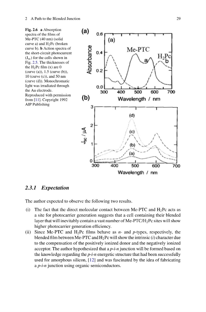
Fig. 2.6 a Absorption
spectra of the films of
Me-PTC (40 nm) (solid
curve a) and H 2 Pc (broken
curve b). b Action spectra of
the short-circuit photocurrent
(J sc ) for the cells shown in
Fig. 2.5. The thicknesses of
the H 2 Pc film (x) are 0
(curve (a)), 1.5 (curve (b)),
10 (curve (c)), and 50 nm
(curve (d)). Monochromatic
light was irradiated through
the Au electrode.
Reproduced with permission
from [11]. Copyright 1992
AIP Publishing
2.3.1 Expectation
The author expected to observe the following two results.
(i) The fact that the direct molecular contact between Me-PTC and H 2 Pc acts as
a site for photocarrier generation suggests that a cell containing their blended
layer that will inevitably contain a vast number of Me-PTC/H 2 Pc sites will show
higher photocarrier generation efficiency.
(ii) Since Me-PTC and H 2 Pc films behave as n- and p-types, respectively, the
blended film between Me-PTC and H 2 Pc will show the intrinsic (i) character due
to the compensation of the positively ionized donor and the negatively ionized
acceptor. The author hypothesized that a p-i-n junction will be formed based on
the knowledge regarding the p-i-n energetic structure that had been successfully
used for amorphous silicon, [12] and was fascinated by the idea of fabricating
a p-i-n junction using organic semiconductors.
29
Fig. 2.6 a Absorption
spectra of the films of
Me-PTC (40 nm) (solid
curve a) and H 2 Pc (broken
curve b). b Action spectra of
the short-circuit photocurrent
(J sc ) for the cells shown in
Fig. 2.5. The thicknesses of
the H 2 Pc film (x) are 0
(curve (a)), 1.5 (curve (b)),
10 (curve (c)), and 50 nm
(curve (d)). Monochromatic
light was irradiated through
the Au electrode.
Reproduced with permission
from [11]. Copyright 1992
AIP Publishing
2.3.1 Expectation
The author expected to observe the following two results.
(i) The fact that the direct molecular contact between Me-PTC and H 2 Pc acts as
a site for photocarrier generation suggests that a cell containing their blended
layer that will inevitably contain a vast number of Me-PTC/H 2 Pc sites will show
higher photocarrier generation efficiency.
(ii) Since Me-PTC and H 2 Pc films behave as n- and p-types, respectively, the
blended film between Me-PTC and H 2 Pc will show the intrinsic (i) character due
to the compensation of the positively ionized donor and the negatively ionized
acceptor. The author hypothesized that a p-i-n junction will be formed based on
the knowledge regarding the p-i-n energetic structure that had been successfully
used for amorphous silicon, [12] and was fascinated by the idea of fabricating
a p-i-n junction using organic semiconductors.