

2 A Path to the Blended Junction
27
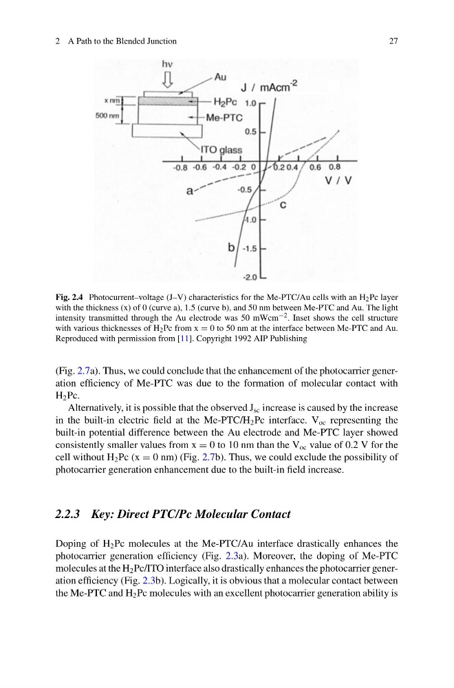
Fig. 2.4 Photocurrent–voltage (J–V) characteristics for the Me-PTC/Au cells with an H 2 Pc layer
with the thickness (x) of 0 (curve a), 1.5 (curve b), and 50 nm between Me-PTC and Au. The light
intensity transmitted through the Au electrode was 50 mWcm −2 . Inset shows the cell structure
with various thicknesses of H 2 Pc from x = 0 to 50 nm at the interface between Me-PTC and Au.
Reproduced with permission from [11]. Copyright 1992 AIP Publishing
(Fig. 2.7a). Thus, we could conclude that the enhancement of the photocarrier generation efficiency of Me-PTC was due to the formation of molecular contact with
H 2 Pc.
Alternatively, it is possible that the observed J sc increase is caused by the increase
in the built-in electric field at the Me-PTC/H 2 Pc interface. V oc representing the
built-in potential difference between the Au electrode and Me-PTC layer showed
consistently smaller values from x = 0 to 10 nm than the V oc value of 0.2 V for the
cell without H 2 Pc (x = 0 nm) (Fig. 2.7b). Thus, we could exclude the possibility of
photocarrier generation enhancement due to the built-in field increase.
2.2.3 Key: Direct PTC/Pc Molecular Contact
Doping of H 2 Pc molecules at the Me-PTC/Au interface drastically enhances the
photocarrier generation efficiency (Fig. 2.3a). Moreover, the doping of Me-PTC
molecules at the H 2 Pc/ITO interface also drastically enhances the photocarrier generation efficiency (Fig. 2.3b). Logically, it is obvious that a molecular contact between
the Me-PTC and H 2 Pc molecules with an excellent photocarrier generation ability is
27
Fig. 2.4 Photocurrent–voltage (J–V) characteristics for the Me-PTC/Au cells with an H 2 Pc layer
with the thickness (x) of 0 (curve a), 1.5 (curve b), and 50 nm between Me-PTC and Au. The light
intensity transmitted through the Au electrode was 50 mWcm −2 . Inset shows the cell structure
with various thicknesses of H 2 Pc from x = 0 to 50 nm at the interface between Me-PTC and Au.
Reproduced with permission from [11]. Copyright 1992 AIP Publishing
(Fig. 2.7a). Thus, we could conclude that the enhancement of the photocarrier generation efficiency of Me-PTC was due to the formation of molecular contact with
H 2 Pc.
Alternatively, it is possible that the observed J sc increase is caused by the increase
in the built-in electric field at the Me-PTC/H 2 Pc interface. V oc representing the
built-in potential difference between the Au electrode and Me-PTC layer showed
consistently smaller values from x = 0 to 10 nm than the V oc value of 0.2 V for the
cell without H 2 Pc (x = 0 nm) (Fig. 2.7b). Thus, we could exclude the possibility of
photocarrier generation enhancement due to the built-in field increase.
2.2.3 Key: Direct PTC/Pc Molecular Contact
Doping of H 2 Pc molecules at the Me-PTC/Au interface drastically enhances the
photocarrier generation efficiency (Fig. 2.3a). Moreover, the doping of Me-PTC
molecules at the H 2 Pc/ITO interface also drastically enhances the photocarrier generation efficiency (Fig. 2.3b). Logically, it is obvious that a molecular contact between
the Me-PTC and H 2 Pc molecules with an excellent photocarrier generation ability is