

9 Parts-Per-Million-Level Doping Effects …
225
9.5.1 Band-Mapping
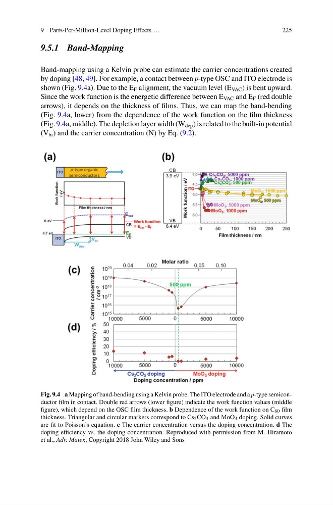
Band-mapping using a Kelvin probe can estimate the carrier concentrations created
by doping [48, 49]. For example, a contact between p-type OSC and ITO electrode is
shown (Fig. 9.4a). Due to the E F alignment, the vacuum level (E VAC ) is bent upward.
Since the work function is the energetic difference between E VAC and E F (red double
arrows), it depends on the thickness of films. Thus, we can map the band-bending
(Fig. 9.4a, lower) from the dependence of the work function on the film thickness
(Fig. 9.4a, middle). The depletion layer width (W dep ) is related to the built-in potential
(V bi ) and the carrier concentration (N) by Eq. (9.2).
Fig. 9.4 a Mapping of band-bending using a Kelvin probe. The ITO electrode and a p-type semiconductor film in contact. Double red arrows (lower figure) indicate the work function values (middle
figure), which depend on the OSC film thickness. b Dependence of the work function on C 60 film
thickness. Triangular and circular markers correspond to Cs 2 CO 3 and MoO 3 doping. Solid curves
are fit to Poisson’s equation. c The carrier concentration versus the doping concentration. d The
doping efficiency vs. the doping concentration. Reproduced with permission from M. Hiramoto
et al., Adv. Mater., Copyright 2018 John Wiley and Sons
225
9.5.1 Band-Mapping
Band-mapping using a Kelvin probe can estimate the carrier concentrations created
by doping [48, 49]. For example, a contact between p-type OSC and ITO electrode is
shown (Fig. 9.4a). Due to the E F alignment, the vacuum level (E VAC ) is bent upward.
Since the work function is the energetic difference between E VAC and E F (red double
arrows), it depends on the thickness of films. Thus, we can map the band-bending
(Fig. 9.4a, lower) from the dependence of the work function on the film thickness
(Fig. 9.4a, middle). The depletion layer width (W dep ) is related to the built-in potential
(V bi ) and the carrier concentration (N) by Eq. (9.2).
Fig. 9.4 a Mapping of band-bending using a Kelvin probe. The ITO electrode and a p-type semiconductor film in contact. Double red arrows (lower figure) indicate the work function values (middle
figure), which depend on the OSC film thickness. b Dependence of the work function on C 60 film
thickness. Triangular and circular markers correspond to Cs 2 CO 3 and MoO 3 doping. Solid curves
are fit to Poisson’s equation. c The carrier concentration versus the doping concentration. d The
doping efficiency vs. the doping concentration. Reproduced with permission from M. Hiramoto
et al., Adv. Mater., Copyright 2018 John Wiley and Sons