

9 Parts-Per-Million-Level Doping Effects …
223
2.0
3.0
4.0
5.0
6.0
7.0
3.87
6.2
C 60 C 70
3.92
6.2
3.5
5.1
H 2 Pc
3.5 3.5
0
.
5
0
.
5
ZnPc CuPc
3.5
5.5
DBP
3.2
5.4
Rubrene
3.2
5.0
Pentacene
4.88
4.19
5.99
4.76
4.36
3.78
4.86
4.53
3.76
4.08
4.54
5.20
3.32
4.69
5.16
3.37
4.53
4.73
5.88
4.60
4.40
4.4
3.76
4.89
6.69
2.96
Cs 2 CO 3
MoO 3
6T
4.83
4.41
3.96
3.1
5.2
Co-deposited film
Electron energy / eV
Single semiconductor films
3.87
6.2
3.5
5.1
H 2 Pc/C 60
4.22
4.48
4.95
Acceptor molecule Donor molecule
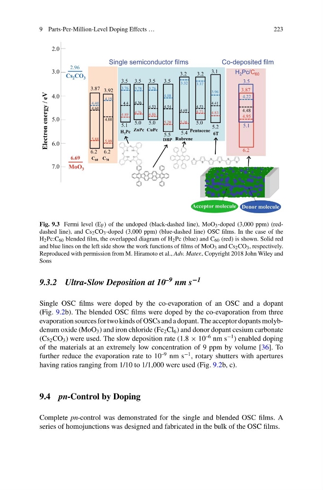
Fig. 9.3 Fermi level (E F ) of the undoped (black-dashed line), MoO 3 -doped (3,000 ppm) (reddashed line), and Cs 2 CO 3 -doped (3,000 ppm) (blue-dashed line) OSC films. In the case of the
H 2 Pc:C 60 blended film, the overlapped diagram of H 2 Pc (blue) and C 60 (red) is shown. Solid red
and blue lines on the left side show the work functions of films of MoO 3 and Cs 2 CO 3 , respectively.
Reproduced with permission from M. Hiramoto et al., Adv. Mater., Copyright 2018 John Wiley and
Sons
9.3.2 Ultra-Slow Deposition at 10 –9 nm s −1
Single OSC films were doped by the co-evaporation of an OSC and a dopant
(Fig. 9.2b). The blended OSC films were doped by the co-evaporation from three
evaporation sources for two kinds of OSCs and a dopant. The acceptor dopants molybdenum oxide (MoO 3 ) and iron chloride (Fe 2 Cl 6 ) and donor dopant cesium carbonate
(Cs 2 CO 3 ) were used. The slow deposition rate (1.8 × 10
–6 nm s
−1 ) enabled doping
of the materials at an extremely low concentration of 9 ppm by volume [36]. To
further reduce the evaporation rate to 10
–9 nm s
−1 , rotary shutters with apertures
having ratios ranging from 1/10 to 1/1,000 were used (Fig. 9.2b, c).
9.4 pn-Control by Doping
Complete pn-control was demonstrated for the single and blended OSC films. A
series of homojunctions was designed and fabricated in the bulk of the OSC films.
223
2.0
3.0
4.0
5.0
6.0
7.0
3.87
6.2
C 60 C 70
3.92
6.2
3.5
5.1
H 2 Pc
3.5 3.5
0
.
5
0
.
5
ZnPc CuPc
3.5
5.5
DBP
3.2
5.4
Rubrene
3.2
5.0
Pentacene
4.88
4.19
5.99
4.76
4.36
3.78
4.86
4.53
3.76
4.08
4.54
5.20
3.32
4.69
5.16
3.37
4.53
4.73
5.88
4.60
4.40
4.4
3.76
4.89
6.69
2.96
Cs 2 CO 3
MoO 3
6T
4.83
4.41
3.96
3.1
5.2
Co-deposited film
Electron energy / eV
Single semiconductor films
3.87
6.2
3.5
5.1
H 2 Pc/C 60
4.22
4.48
4.95
Acceptor molecule Donor molecule
Fig. 9.3 Fermi level (E F ) of the undoped (black-dashed line), MoO 3 -doped (3,000 ppm) (reddashed line), and Cs 2 CO 3 -doped (3,000 ppm) (blue-dashed line) OSC films. In the case of the
H 2 Pc:C 60 blended film, the overlapped diagram of H 2 Pc (blue) and C 60 (red) is shown. Solid red
and blue lines on the left side show the work functions of films of MoO 3 and Cs 2 CO 3 , respectively.
Reproduced with permission from M. Hiramoto et al., Adv. Mater., Copyright 2018 John Wiley and
Sons
9.3.2 Ultra-Slow Deposition at 10 –9 nm s −1
Single OSC films were doped by the co-evaporation of an OSC and a dopant
(Fig. 9.2b). The blended OSC films were doped by the co-evaporation from three
evaporation sources for two kinds of OSCs and a dopant. The acceptor dopants molybdenum oxide (MoO 3 ) and iron chloride (Fe 2 Cl 6 ) and donor dopant cesium carbonate
(Cs 2 CO 3 ) were used. The slow deposition rate (1.8 × 10
–6 nm s
−1 ) enabled doping
of the materials at an extremely low concentration of 9 ppm by volume [36]. To
further reduce the evaporation rate to 10
–9 nm s
−1 , rotary shutters with apertures
having ratios ranging from 1/10 to 1/1,000 were used (Fig. 9.2b, c).
9.4 pn-Control by Doping
Complete pn-control was demonstrated for the single and blended OSC films. A
series of homojunctions was designed and fabricated in the bulk of the OSC films.