

In the example shown in Figure 4.23, a direct write lithographic technique, dip
pen lithography [158, 159], which relies on a cantilever used for atomic force
microscopy (AFM) to write on a substrate to create patterns of Au nanocrystals
on mica substrates. Thus, nanocrystals of metals and semiconductors can be patterned into rectangles of varying aspect ratios.
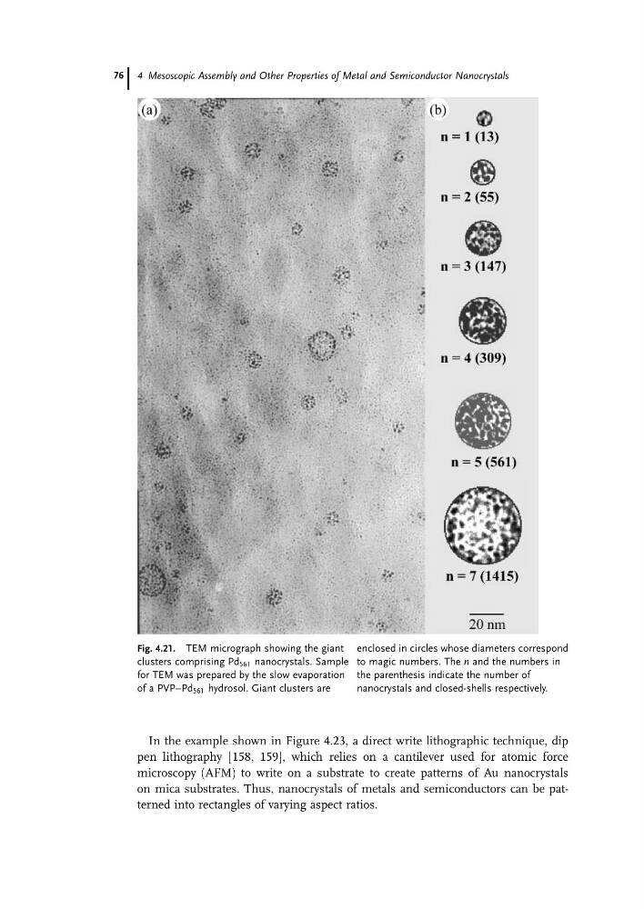
Fig. 4.21. TEM micrograph showing the giant
clusters comprising Pd 561 nanocrystals. Sample
for TEM was prepared by the slow evaporation
of a PVP–Pd 561 hydrosol. Giant clusters are
enclosed in circles whose diameters correspond
to magic numbers. The n and the numbers in
the parenthesis indicate the number of
nanocrystals and closed-shells respectively.
4 Mesoscopic Assembly and Other Properties of Metal and Semiconductor Nanocrystals
76
pen lithography [158, 159], which relies on a cantilever used for atomic force
microscopy (AFM) to write on a substrate to create patterns of Au nanocrystals
on mica substrates. Thus, nanocrystals of metals and semiconductors can be patterned into rectangles of varying aspect ratios.
Fig. 4.21. TEM micrograph showing the giant
clusters comprising Pd 561 nanocrystals. Sample
for TEM was prepared by the slow evaporation
of a PVP–Pd 561 hydrosol. Giant clusters are
enclosed in circles whose diameters correspond
to magic numbers. The n and the numbers in
the parenthesis indicate the number of
nanocrystals and closed-shells respectively.
4 Mesoscopic Assembly and Other Properties of Metal and Semiconductor Nanocrystals
76