

means of obtaining robust structures involves multilayer deposition of nanocrystals and has been drawing a great deal of attention over the last few years, since
it provides a convenient, low-cost means to prepare ultra-thin films of controlled
thickness, suitable for device applications. In a typical experiment, one end of a
monolayer forming bifunctional spacer, is tethered to a flat substrate such as gold,
aluminum, indium tin oxide or glass, leaving the other end free to anchor nano2
4
6
8
r (nm)
2
4
6
8
r (nm)
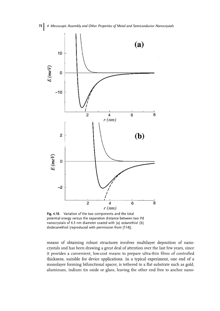
Fig. 4.18. Variation of the two components and the total
potential energy versus the separation distance between two Pd
nanocrystals of 4.5 nm diameter coated with (a) octanethiol (b)
dodecanethiol (reproduced with permission from [114]).
4 Mesoscopic Assembly and Other Properties of Metal and Semiconductor Nanocrystals
72
it provides a convenient, low-cost means to prepare ultra-thin films of controlled
thickness, suitable for device applications. In a typical experiment, one end of a
monolayer forming bifunctional spacer, is tethered to a flat substrate such as gold,
aluminum, indium tin oxide or glass, leaving the other end free to anchor nano2
4
6
8
r (nm)
2
4
6
8
r (nm)
Fig. 4.18. Variation of the two components and the total
potential energy versus the separation distance between two Pd
nanocrystals of 4.5 nm diameter coated with (a) octanethiol (b)
dodecanethiol (reproduced with permission from [114]).
4 Mesoscopic Assembly and Other Properties of Metal and Semiconductor Nanocrystals
72