

11.7
Concluding Remarks
We have reviewed in this chapter the electronic structure and properties of semiconducting nanocrystals, materials that can be used in the field of nanoelectronics
in the near future. Some of these materials already show very interesting properties that can be utilized to make devices and, therefore, it is necessary to have
proper experimental and theoretical tools to probe and understand the electronic
properties quantitatively.
UV–Vis absorption spectroscopy is the easiest tool available to characterize semi0
102
03
0
405
06
07
0
-1.6
-1.4
-1.2
-1.0
-0.8
-0.6
-0.4
-0.2
0.0
0.2
0.4
0.6
0.8
1.0
1.2
1.4
1.6
1.8
BCB
TVB
Energy (eV)
Diameter (Å)
theory
experiment
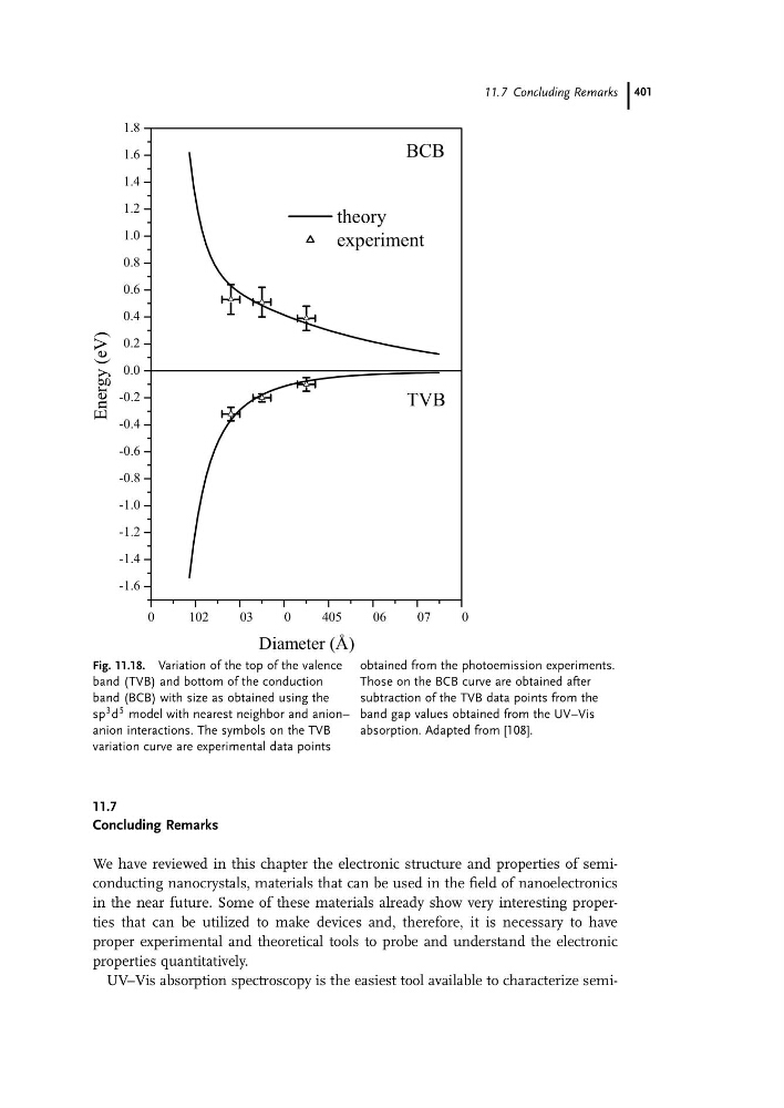
Fig. 11.18. Variation of the top of the valence
band (TVB) and bottom of the conduction
band (BCB) with size as obtained using the
sp
3 d
5 model with nearest neighbor and anion–
anion interactions. The symbols on the TVB
variation curve are experimental data points
obtained from the photoemission experiments.
Those on the BCB curve are obtained after
subtraction of the TVB data points from the
band gap values obtained from the UV–Vis
absorption. Adapted from [108].
11.7 Concluding Remarks 401
Concluding Remarks
We have reviewed in this chapter the electronic structure and properties of semiconducting nanocrystals, materials that can be used in the field of nanoelectronics
in the near future. Some of these materials already show very interesting properties that can be utilized to make devices and, therefore, it is necessary to have
proper experimental and theoretical tools to probe and understand the electronic
properties quantitatively.
UV–Vis absorption spectroscopy is the easiest tool available to characterize semi0
102
03
0
405
06
07
0
-1.6
-1.4
-1.2
-1.0
-0.8
-0.6
-0.4
-0.2
0.0
0.2
0.4
0.6
0.8
1.0
1.2
1.4
1.6
1.8
BCB
TVB
Energy (eV)
Diameter (Å)
theory
experiment
Fig. 11.18. Variation of the top of the valence
band (TVB) and bottom of the conduction
band (BCB) with size as obtained using the
sp
3 d
5 model with nearest neighbor and anion–
anion interactions. The symbols on the TVB
variation curve are experimental data points
obtained from the photoemission experiments.
Those on the BCB curve are obtained after
subtraction of the TVB data points from the
band gap values obtained from the UV–Vis
absorption. Adapted from [108].
11.7 Concluding Remarks 401