

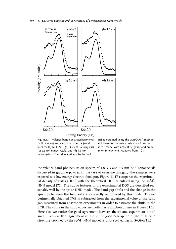
the valence band photoemission spectra of 1.8, 2.5 and 3.5 nm ZnS nanocrystals
dispersed in graphite powder. In the case of excessive charging, the samples were
exposed to a low energy electron floodgun. Figure 11.17 compares the experimental density of states (DOS) with the theoretical DOS calculated using the sp
3 d
5 -
NNN model [75]. The subtle features in the experimental DOS are described reasonably well by the sp
3 d
5 -NNN model. The band gap shifts and the change in the
spacings between the two peaks are correctly reproduced by this model. The experimentally obtained TVB is subtracted from the experimental value of the band
gap measured from absorption experiments in order to estimate the shifts in the
BCB. The shifts in the band edges are plotted as a function of size in Figure 11.18.
Here also we notice the good agreement between theory and experiment for all
sizes. Such excellent agreement is due to the good description of the bulk band
structure provided by the sp
3 d
5 -NNN model as discussed earlier in Section 11.5.
86420
86420
Binding Energy (eV)
(a) bulk
Theory
Experiment
Intensity (arb. units)
LMTO-ASA
Valence Band
(b) 3.5 nm
(c) 2.5 nm
(d) 1.8 nm
Fig. 11.17. Valence band spectra:experimental
(solid circles) and calculated spectra (solid
line) for (a) bulk ZnS, (b) 3.5 nm nanocrystals,
(c) 2.5 nm nanocrystals, and (d) 1.8 nm
nanocrystals. The calculated spectra for bulk
ZnS is obtained using the LMTO-ASA method
and those for the nanocrystals are from the
sp
3 d
5 model with nearest neighbor and anionanion interactions. Adapted from [108].
11 Electronic Structure and Spectroscopy of Semiconductor Nanocrystals
400
dispersed in graphite powder. In the case of excessive charging, the samples were
exposed to a low energy electron floodgun. Figure 11.17 compares the experimental density of states (DOS) with the theoretical DOS calculated using the sp
3 d
5 -
NNN model [75]. The subtle features in the experimental DOS are described reasonably well by the sp
3 d
5 -NNN model. The band gap shifts and the change in the
spacings between the two peaks are correctly reproduced by this model. The experimentally obtained TVB is subtracted from the experimental value of the band
gap measured from absorption experiments in order to estimate the shifts in the
BCB. The shifts in the band edges are plotted as a function of size in Figure 11.18.
Here also we notice the good agreement between theory and experiment for all
sizes. Such excellent agreement is due to the good description of the bulk band
structure provided by the sp
3 d
5 -NNN model as discussed earlier in Section 11.5.
86420
86420
Binding Energy (eV)
(a) bulk
Theory
Experiment
Intensity (arb. units)
LMTO-ASA
Valence Band
(b) 3.5 nm
(c) 2.5 nm
(d) 1.8 nm
Fig. 11.17. Valence band spectra:experimental
(solid circles) and calculated spectra (solid
line) for (a) bulk ZnS, (b) 3.5 nm nanocrystals,
(c) 2.5 nm nanocrystals, and (d) 1.8 nm
nanocrystals. The calculated spectra for bulk
ZnS is obtained using the LMTO-ASA method
and those for the nanocrystals are from the
sp
3 d
5 model with nearest neighbor and anionanion interactions. Adapted from [108].
11 Electronic Structure and Spectroscopy of Semiconductor Nanocrystals
400