

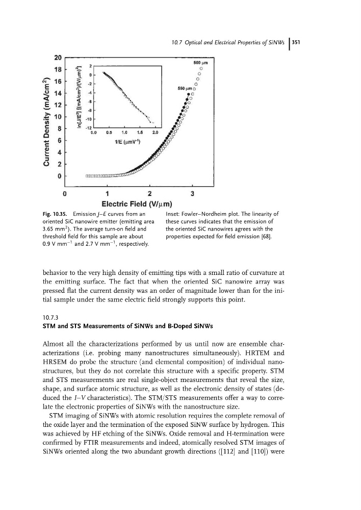
behavior to the very high density of emitting tips with a small ratio of curvature at
the emitting surface. The fact that when the oriented SiC nanowire array was
pressed flat the current density was an order of magnitude lower than for the initial sample under the same electric field strongly supports this point.
10.7.3
STM and STS Measurements of SiNWs and B-Doped SiNWs
Almost all the characterizations performed by us until now are ensemble characterizations (i.e. probing many nanostructures simultaneously). HRTEM and
HRSEM do probe the structure (and elemental composition) of individual nanostructures, but they do not correlate this structure with a specific property. STM
and STS measurements are real single-object measurements that reveal the size,
shape, and surface atomic structure, as well as the electronic density of states (deduced the I–V characteristics). The STM/STS measurements offer a way to correlate the electronic properties of SiNWs with the nanostructure size.
STM imaging of SiNWs with atomic resolution requires the complete removal of
the oxide layer and the termination of the exposed SiNW surface by hydrogen. This
was achieved by HF etching of the SiNWs. Oxide removal and H-termination were
confirmed by FTIR measurements and indeed, atomically resolved STM images of
SiNWs oriented along the two abundant growth directions ([112] and [110]) were
Fig. 10.35. Emission J–E curves from an
oriented SiC nanowire emitter (emitting area
3.65 mm
2 ). The average turn-on field and
threshold field for this sample are about
0.9 V mm
À1 and 2.7 V mm
À1 , respectively.
Inset: Fowler–Nordheim plot. The linearity of
these curves indicates that the emission of
the oriented SiC nanowires agrees with the
properties expected for field emission [68].
10.7 Optical and Electrical Properties of SiNWs 351
the emitting surface. The fact that when the oriented SiC nanowire array was
pressed flat the current density was an order of magnitude lower than for the initial sample under the same electric field strongly supports this point.
10.7.3
STM and STS Measurements of SiNWs and B-Doped SiNWs
Almost all the characterizations performed by us until now are ensemble characterizations (i.e. probing many nanostructures simultaneously). HRTEM and
HRSEM do probe the structure (and elemental composition) of individual nanostructures, but they do not correlate this structure with a specific property. STM
and STS measurements are real single-object measurements that reveal the size,
shape, and surface atomic structure, as well as the electronic density of states (deduced the I–V characteristics). The STM/STS measurements offer a way to correlate the electronic properties of SiNWs with the nanostructure size.
STM imaging of SiNWs with atomic resolution requires the complete removal of
the oxide layer and the termination of the exposed SiNW surface by hydrogen. This
was achieved by HF etching of the SiNWs. Oxide removal and H-termination were
confirmed by FTIR measurements and indeed, atomically resolved STM images of
SiNWs oriented along the two abundant growth directions ([112] and [110]) were
Fig. 10.35. Emission J–E curves from an
oriented SiC nanowire emitter (emitting area
3.65 mm
2 ). The average turn-on field and
threshold field for this sample are about
0.9 V mm
À1 and 2.7 V mm
À1 , respectively.
Inset: Fowler–Nordheim plot. The linearity of
these curves indicates that the emission of
the oriented SiC nanowires agrees with the
properties expected for field emission [68].
10.7 Optical and Electrical Properties of SiNWs 351