

the substrate, leading to condensation of droplets when the substrate temperature
is lower than the melting point of the metal silicide clusters. The melting point of
the nanoclusters decreases with decreasing size in the nanometer region. Large
droplets will melt and serve as SiNW nucleation sites at higher temperatures than
small droplets, explaining the decrease in the SiNW diameter with decreasing
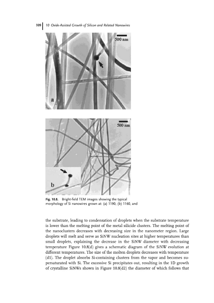
temperature Figure 10.8(d) gives a schematic diagram of the SiNW evolution at
different temperatures. The size of the molten droplets decreases with temperature
(d1). The droplet absorbs Si-containing clusters from the vapor and becomes supersaturated with Si. The excessive Si precipitates out, resulting in the 1D growth
of crystalline SiNWs shown in Figure 10.8(d2) the diameter of which follows that
Fig. 10.8. Bright-field TEM images showing the typical
morphology of Si nanowires grown at: (a) 1190, (b) 1160, and
10 Oxide-Assisted Growth of Silicon and Related Nanowires
320
is lower than the melting point of the metal silicide clusters. The melting point of
the nanoclusters decreases with decreasing size in the nanometer region. Large
droplets will melt and serve as SiNW nucleation sites at higher temperatures than
small droplets, explaining the decrease in the SiNW diameter with decreasing
temperature Figure 10.8(d) gives a schematic diagram of the SiNW evolution at
different temperatures. The size of the molten droplets decreases with temperature
(d1). The droplet absorbs Si-containing clusters from the vapor and becomes supersaturated with Si. The excessive Si precipitates out, resulting in the 1D growth
of crystalline SiNWs shown in Figure 10.8(d2) the diameter of which follows that
Fig. 10.8. Bright-field TEM images showing the typical
morphology of Si nanowires grown at: (a) 1190, (b) 1160, and
10 Oxide-Assisted Growth of Silicon and Related Nanowires
320